 UPDATE HISTORY:
- Oct 29 2024 - Documented AIBO sticks
- May 17 2022 - Documented the Sony Memory Stick Host chip MB86189
- Apr 4 2022 - Added MSIO Camera documentation, added camera and GPS sample code
- Apr 3 2022 - Added MSIO GPS documentation
- Mar 25 2022 - Added some more MSIO info
- Mar 19 2022 - added some MSIO info
Disclaimer: most of this data was scrounged from many sources, guessed from disassembly, inferred from strings or documents, or obtained by participating in demonic rituals. It might be slightly wrong, it might be completely wrong, it might kill your cat, and it might break your car. No promises are made that any of the abovementioned consequenced may or may not happen to you or your cat.
Table of Contents
- The field
- The basics
- Talking to Memory Sticks
- Memory Stick Classic
- Memory Stick Pro
- Memory Stick IO
- The Chip
- Code for download
- Comments...
The field
Much has been written about how to talk to SD cards. The spec is somewhat available, and the SPI mode, while optional, is basically always present. Interfacing a microcontroller to an SD card is about as much a non-event as interfacing anything to anything can be. MMC cards are basically the same thing, minus a few command differences that are trivial to account for. Compact Flash is basically IDE, which is basically ISA. Also, it requires more pins than most people care to connect to a microcontroller, so pretty much nobody cares about interfacing to CF. SmartMedia/xD is so dead, that I feel like a necromancer even mentioning it. So what memory card format does this leave? The alive-until-somewhat-recently Memory Stick, of course!
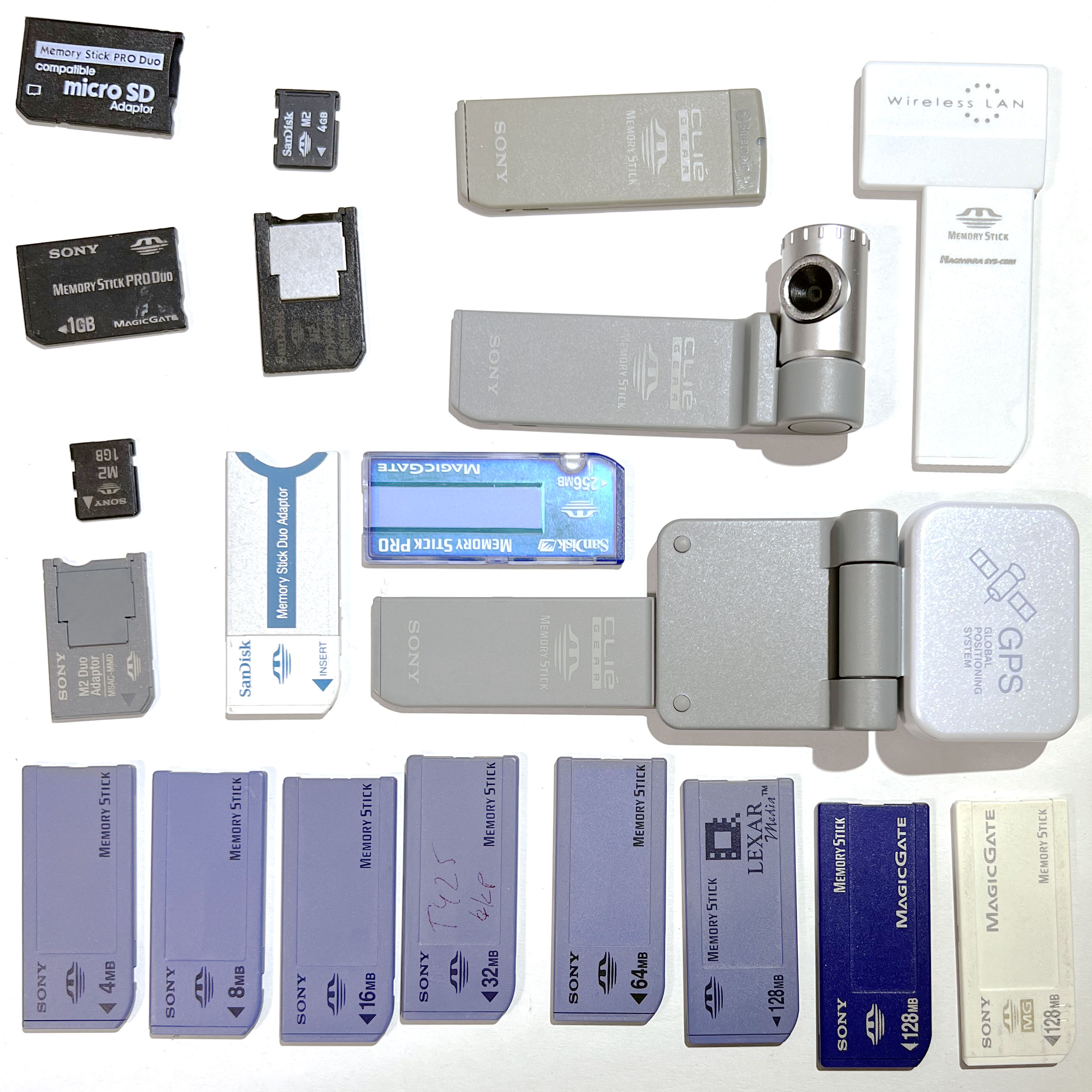
The cards came in a number of varieties, the differences between which were never quite clearly explained, of course. There were the normal blue Memory Sticks in sizes from 4MB to 128MB. There were Pink Aibo Memory Sticks, which were necessary to use Sony's Aibo robot dogs. These go for hundreds of dollars on eBay nowadays, as there is no more supply. There were white and purple Magic Gate memory sticks in 32 - 128MB sizes. Magic Gate was Sony's DRM technology, similar in design to SD's DRM; a similar number of users (zero) seriously cared about this. There was MSIO - a method to attach non-memory devices with a Memory Stick slot, similar to SDIO. There were Memory Stick cameras, GPS devices, Bluetooth radios, and WiFi cards. Then, there was the size-reduced Memory Stick DUO which was half the size and came with an adapter to "full-size" it for devices that needed a full-sized Memory Stick. Then there was also Memory Stick Pro, in sizes from 256MB to 2GB, and of course Pro DUO existed as well. All of those also came in Magic Gate varieties as well as not. Later, there was a Memory Stick PRO HG, which was slightly smaller yet, necessitating more adapters, slightly faster when used with devices that supported it, and supported by literally no devices in existence. This one also supported an 8-bit-wide data transfer mode that I have seen no evidence of in any product. As a final death throe, there was also The Memory Stick Micro (also known as M2) which was about the size of a MicroSD card. Electrically this was a Memory Stick Pro (optionally with Magic Gate, of course) in a smaller size. These came with TWO adapters that nested, if needed, to convert it to a full size Memory Stick or a half-size Memory Stick DUO. Sony announced a few more versions: Memory Stick XC and Memory Stick Pro HG Duo XC. No I am not making this up! Just rolls off the tongue, doesn't it? Luckily, as far as I can tell, neither of those last two Memory sticks ever materialized. Phew...
Why do we care?
Well, preserving history, for one. But also because reverse engineering things is fun? Plus now you can use memory sticks in your microcontroler projects (if you manage to find a proper adapter). My work focused on Memory Stick storage and I did not spend too much time on MSIO, but there is some info here on that too.
The basics
What we know
From what public information is available, and from simple tear downs of devices that use Memory Sticks, we can gather some basic info: Each card has 10 pins (HG has more, but nobody cares). Two of them are ground, one is used for insertion detection only and is tied to ground in the stick, and one supplies power. This leaves us with 6 pins for data transfer. Some more research indicates that there was a 4-bit-wide mode that used 6 pins and a 1-bit-wide mode that used 3. The pinout is public, actually. Seems sane. What now?
I started the analysis with my old Sony CLIE handhelds. It is a simple, familiar environment, and based on the wiring it was clear that they used the simpler 1-bit mode. It also helps that due to the way PalmOS 4 binaries were built, many of them retain function names in the binary. In addition, despite being a godawful architecture, 68k is easy to reverse engineer since a lot more type info is available than in ARM binaries. Some logic analyzer capturing took place as well. After a few days, I had a working basic interface to a memory stick and some names put to concepts.
Gross...
Ok, so first things first: whoever came up with this physical layer protocol was a sadist. There is no other way around this. A few things make me say this. First of all: when you want to signal that you are busy, or ready, most sane designs use one level for one, one for another. For example, SD cards will keep the data line low while they are busy, and it is high when they are not. Well, not Sony. Oh no! When the card is ready to continue communicating it will transmit bytes 0xAA or 0x55 on the line. Because of course that makes sense! But that is not all! There is a signal called Bus State, that toggles between phases of communication (approximately: command, handshake, data, and ack). Good so far? Here's a curveball: it toggles one bit BEFORE any given phase is over. So the last bit of any given phase is sent after it has toggled. Why? Probably just to make my life harder. Sony tightly controlled Memory Stick interfaces. The only way to make a host device was to use a Sony chip or a SoC that had Memory Stick support built-in, which was an IP block licenseable from Sony only. This tight control freed them from anyone sane ever looking into their design, giving them a strong shake, and committing them to an insane asylum. But I digress...
Talking to Memory Sticks
The Physical layer
The physical layer of the 1-bit-wide mode is three wires: BS wire to signal bus state, CLK wire for the host to send the card a clock signal (20MHz is every device I've inspected, but lower speeds all work perfectly, down to DC), and SDIO for bidirectional data. In 4-bit-wide mode the only change is that SDIO becomes DATA0, and DATA1, DATA2, DATA3 join the fray. Also the clock is now 40MHz. Data is always sent MSB first and all parts of every transaction on the wire are byte-sized.
Data line(s) should be pulled down. As the data line(s) are bidirectional, they need time to switch direction. There is always a bit's worth of clock time to do that! Clock idles low. Data is latched on the rising edge both by host and by card.
Transactions
The lowest level of communication with Memory Stick is a transaction (Sony calls it a TPC). I do not know what the term means, so i'll go ahead and guess that it is a Transfer/Protocol/Command. Like I said, PalmOS 4.0 binaries give us function names only. In any case, every TPC has an 8-bit code, the bottom 4 of which are the inverse of the top four. A way to make sure they were transferred correctly, I guess. Unlike SD commands, each and every TPC includes a unidirectional data transfer. The top bit of the TPC determines the direction: high means write, low means read. The amount of data transferred is not directly sent, it is implied by previous settings or the TPC itself. The data is always followed by a 16-bit CRC, big endian, starting value 0x0000, poly 0x8005. Unlike SD, where in 4-bit mode each line gets its own CRC, here a single CRC is sent, over 4 lines (much more efficient). The maximum number of bytes transferred by a single TPC is 512, the minimum is one (plus two CRC bytes, always).
Here is how a transaction with a host-to-card data transfer goes. BS goes high. This means that in one bit's time, TPC will be sent. But first, a bit is sent with no meaning. Then the 4 bits of the TPC are sent. Next we'll need to send the 4 bits of TPC inverted, but remember that sadistic thing about the BS signal flipping early? So, we send the top 3 bits of inverted TPC, and then BS goes low and we send the last bit. Now we're in the data phase. We clock out data now, one bit at a time. After the data, we send the MSB of the CRC as a byte. Then would come the LSB, but, again, that sadistic one-bit-before-its-time BS switch needs to happen, so we send the top 7 bits of the CRC's LSB, then BS goes high again, and then we send the last bit. At this point we're in the handshaking stage. We switch the SDIO line into receive mode, and start sending clocks. When we notice the Memory Stick sending us 0x55 or 0xAA, we've received the handshake and we flip BS back to low and we're done. If, after an adequate wait time, we do not receive a handshake, the card was unhappy with us and we need to retry. This will happen due to an invalid TPC, mismatched inverted TPC, or a data CRC error.
A transaction with a card-to-host transfer is somewhat similar. The TPC and its inverse are sent the same way, then we switch SDIO line into receive mode and wait for handshaking, same as explained above. Again, a timeout here is used to avoid waiting forever. Once handshaking is noted, we flip BS line high and enter the data phase. Same as before, BS-flips-one-bit-too-early gets us, and we need to clock out an extra bit to give the card a chance to finish its handshake. After this we begin receiving data bytes, and then the CRC. As before, we need to flip BS line low one bit before the CRC is over, but it seems that most cards do not care if you do it later, which is simpler.
Registers
Memory Stick has a number of registers which configure things like accessed memory, modes, etc. They are accessed using a register window. There is a TPC SET_REGS_WINDOW (0b1000) that sets the read and write register window start and length values. This TPC always comes with 4 bytes of data: start read register, num read registers, start write register, num write registers. Then those settings determine the number of bytes expected or sent for REGS_WRITE (0b1011) and REGS_READ (0b0100) TPCs, respectively. Commands to the memory stick are issued used a SET_CMD (0b1110) TPC, and for Memory Stick Pro there is also a shortcut to combine setting some regs and sending a command in the form of SET_CMD_EX (0b1001) TPC. Data transfer is done using READ_LONG_DATA (0b0010) to read 512 bytes, and WRITE_LONG_DATA (0b1101) to write 512 bytes. The INT register which contains the most useful status bits can also be read directly using the GET_INT (0b0111) TPC that returns one byte as data. There are also TPCs to read/write less than 512 bytes of data to the stick, but those seem to only be used for MSIO. They are READ_SHORT_DATA (0b0011) and WRITE_SHORT_DATA (0b1100). The actual length is set by a register, with options for 32, 64, 128, and 256 bytes, as per disassembly of existing code.
Commands
Commands are sent using SET_CMD with one byte of data - the command code. Memory Stick Pro also has another way, but more on that later. You send a command, what then? You read the INT register using either GET_INT or REGS_READ until bit 0x80 goes high. This means command is completed. For commands that do data transfer, bit 0x20 might go up instead. This means that the stick is ready for data transfer. Bit 0x40 means an error occured. Commands use parameters that you need to pre-write to registers. Data is written to the card using WRITE_LONG_DATA when card expects it, and read from card using READ_LONG_DATA when card is ready to provide it as per INT. Some devices (eg: PEG-NR70) expect a device to be ready for further TPCs after sending a commany by 39us after the command ends. Not fun...
Screech...*sound of breaking glass*
This is where we find our first surprise. Memory Stick (which i'll refer to as "Classic") is *ENTIRELY* different from Memory Stick Pro (henceforth known as "Pro"). And I do not mean "slightly different", or "somewhat different". Entirely different! The registers are different, the accepted commands are different, and data layout is different. Since PalmOS 4.0 devices only supported Memory Stick Classic, we'll cover them first. (Plot twist: as a branch from this work, I went ahead and added Memory Stick Pro support to some PalmOS 3.5 and 4.0 Sony CLIE devices by binary patching their existing Memory Stick drivers and adding a few kilobytes of code hooked into all the right places);
Memory Stick Classic
Register summary (classic)
| ADDRESS | NAME | USE |
|---|---|---|
| 0x01 | INT | Card interrupt - the most direct status there is. Tells us when the card is done with an operation, when an error has occured, when card is ready for data, etc. |
| 0x02 | STA0 | Status 0 - more status bits. Bit 0 here is set if the stick is write protected. Bit 1 is set when Memory Stick sleeps. |
| 0x03 | STA1 | Status 1 - more status yet. Here we'll be able to read NAND error correction status. More on them later. |
| 0x04 | TYPE | Stick type. Classic will have 0xff here. Pro will have 0x01. MSIO will have 0x00 |
| 0x06 | CATEGORY | Stick subtype. Classic will have 0xff here. Pro will have 0x00. MSIO is special... |
| 0x07 | CLASS | Memory subtype. Classic will have 0xff here. Pro will have 0x00. ROM sticks will have 0x01 |
| 0x10 | CFG | Top bit set will switch to 1-bit-wide mode. Clearing it will switch to 4-bit-wide mode. |
| 0x11 | BLK_HI | High byte of the NAND block index |
| 0x12 | BLK_MID | Middle byte of the NAND block index |
| 0x13 | BLK_LO | Low byte of the NAND block index |
| 0x14 | ACCESSTYP | Specifies details for some commands. More on this later. |
| 0x15 | PAGE | NAND page index |
| 0x16 | OOB[0] | OOB[0] byte |
| 0x17 | OOB[1] | OOB[1] byte |
| 0x18 | OOB[2] | OOB[2] byte |
| 0x19 | OOB[3] | OOB[3] byte |
| 0x1A | OOB[4] | OOB[4] byte |
| 0x1B | OOB[5] | OOB[5] byte |
| 0x1C | OOB[6] | OOB[6] byte |
| 0x1D | OOB[7] | OOB[7] byte |
| 0x1E | OOB[8] | OOB[8] byte |
INT register
This is the main status of the Memory Stick. Bit 7 is "command completed". Bit 6 is "error occured". Bit 5 is "ready for data transfer". Bit 0 is "invalid command". Combinations of them mean precisely what you'd guess given the combinations. Attempting a READ_LONG_DATA or WRITE_LONG_DATA when bit 5 is not set will be ignored. This is the register returned by GET_INT
When card is in idle bus state (between transactions, while BS is low) and in 4-bit-wide mode, it outputs the status of INT register's 4 useful bits on the data lines. Bit 7 is seen on DATA0, bit 6 on DATA1, and bit 5 on DATA2, bit 0 on DATA3. This is why in 4-bit-wide mode, GET_INT is not useful. It does, however, still work. In 1-bit-mode, in the idle bus state SDIO shows the logical-OR of those bits, and acts as the interrupt request to the host, telling it a command is done (since at least one of the INT bits will be set by command completion). Figuring out how it went does require actually reading the INT register, though.
STA1
Here we can read the error correction statusses after a read command. Bits 0, 2, and 4 signal uncorrectable errors (in config data, oob data, and user data) respectively. Bits 1, 3, and 5 signal correctible errors in the same things. Pretty simple. The built-in error correction is able to correct one bit in the user data area and guarantees detection of 2 bitflips. Same for OOB data.
ACCESSTYP
Here we control read and write commands. Setting it to 0x00 will read/write pages sequentially until reaching the end of the block. Error correction will be calculated and written on write, calculated and applied on read. Setting this to 0x20 will only operate on a single page. Error correction will also be calculated/written/applied. Writing 0x40 here also operates on a single page, but the user data area will not be operated on, only the OOB will be read/written. Error correction is still calculated/written/applied. 0x80 is similar, except no error correction is read/written. Only OOB is affected.
For erase operations, this must be set to 0x20
Theory of operation
As you may have guessed from the information above, Memory Stick Classic is just raw NAND with extra steps. The NAND used has 512 - 8192 blocks of 16 or 32 pages of 512 + 16 bytes. Error correction is handled internally by the memory stick controller, leaving 512+9 error corrected bytes available externally. The command set is basically what you'd expect of a NAND device - read/write page, erase block.
Of course, NAND requires wear leveling and bad block management. To remain cross-compatible with other products using Memory Stick, all products must do it precisely the same way. I guess that that is exactly what Sony specified. All devices I opened and captured commands from exhibited the exact same access patterns for stick insertion, read, and write. I'll outline the basics of how it works now. This is based on the PalmOS 4.0 Memory Stick Classic driver, which was small enough to easily completely analyze.
NAND
The NAND is managed in pieces called "segments". Each segment is made of 512 blocks of NAND. The minimum number of segments supported in a Memory Stick Classic is one, the maximum is 16. Since Memory Stick's implementation of flash wear leveling only supports NAND with 16 or 32 pages per block, we thus have the minimum memory stick size: 1 segment of 512 blocks of 16 pages of 512 bytes = 4M. On the maximum side: 16 segments of 512 blocks of 32 pages of 512 bytes = 128M. Curiously, there is nothing at all that stops this flash wear leveling layer from supporting larger NAND devices. The addressing used can, in theory, scale all the way to 128 segments, producing a theretical 1GB Memory Stick Classic. But this was not meant to be. PalmOS Memory Stick driver rejects any Memory sticks claiming to have more than 8192 NAND flash blocks. Sony cameras do as well.
Flash has a tendency to occasionally get a bit wrong here and there. Using flash requires use of error correcting codes (ECC) to avoid losing precious data. Sony Memory Stick Classic devices all used SLC flash with a rather large cell size. This is rather reliable and does not require too much error correction ability. Memory Stick uses ECC that can correct any one wrong bit in a 512-byte page, and detect any too bits flipped. If more bits flipped, detection is not guaranteed but it is likely. This ECC code occupies 3 bytes in the 16-bytes-per-page spare area of the NAND. These bytes are invisible to the Memory Stick host device. The nine host-usable extra per-page data bytes are also corrected similarly.
NAND devices also have bad blocks - blocks that are unable to store data properly. Devices are often shipped form the factory with a few bad blocks already, and more develop over time as NAND is worn by use. Every erase and write operation wears at NAND a little, until it ceases to work. This means that one needs to employ some algorithm to work around the existence of bad blocks and keep track of new ones. This sort of thing is called wear leveling and it is very importatnt to all flash storage. Memory Stick stores the list of initial bad blocks from the factory in the Boot Block and in the Backup Boot Block. New bad blocks are never added there, instead they are marked in the OOB of the first page of the block itself.
To map logical addresses to physical blocks, a translation table is used. To allow for blocks to go bad without the user knowing, 3.125% of the device's raw capacity is hidden from the user and used internally for wear leveling and remapping of blocks. If any segment of a Memory Stick runs out of these reserved blocks (16 per segment initially), the memory stick will enter a permanently-read-only "worn out" state where it can be read but not written. Curiously, with some cleverness, one could still write to other segments, but this is of dubious value, since the segment most likely to go bad is the first - the one containing the FAT12/FAT16 FAT and root directory. Lacking ability to write there almost completely eliminates any reason at all to use the Memory Stick. Of course one could also erase all the blocks in segment zero, write a new partition table skipping the rest of segment zero blocks, and prolong the life of a stick this way, but I digress...
Mapping
Memory is mapped at block granularity. This means that on some Memory Stick Classic devices, the minimum writeable unit is 8KB, and on some it is 16KB. They are usually formatted such that this lines up with FAT12/FAT16 clusters. As long as you only write aligned to those boundaries, all is good. But what if you do not? The Memory Stick driver in your device will have to read the current surrounding sectors next to the one(s) you wrote and then re-write the entire block. Yes, this means that if you write a Memory Stick one sector at a time, you'll cause 16x - 32x as much flash wear than if you write a cluster at a time.
"Wait a second!" you might say, "isn't threre still an area of a FAT12/16 filesystem that is accessed a LOT and one sector at a time?" Yup. The FAT. And Memory Stick has no special provisions to handle that. The only two Memory Sticks I've seen that reached the "worn out - read only" stage did so due to bad block exhaustion in segment zero where the FAT lives. Bad Sony! Very bad Sony!
The commands (classic)
The commands are:
| CMD | VALUE | NOTES |
|---|---|---|
| READ | 0xAA | Read a page or a sequence of pages until stopped by a STOP command. Params are in the registers for block index, page index, and access type |
| PROGRAM | 0x55 | Program a page or a sequence of pages until stopped by a STOP command. Params are in the registers for block index, page index, and access type |
| ERASE | 0x99 | Erase a block. Params are in the registers for block index |
| STOP | 0x33 | End a multi-page READ or a WRITE that is ongoing |
| RESET | 0x3c | Reset the controller |
Mounting a Memory Stick
The basics
When a Memory Stick Classic is inserted, a process is run to "mount" it. What does this mean? Basically, a table is built of where each logical block is stored on the media, and lists are built of bad blocks and free blocks. However, before any of that is done, the geometry of the device must be obtained. On a raw NAND device there is usually a command for that. Nowadays there is even a spec (ONFI) for how NAND devices can be discovered and identified by a host that starts out knowing nothing. Well, Sony is not nearly this nice. There are no commands to discover the raw geometry of the NAND inside a memory stick.
Memory Stick Classic stores all per-device management info in the Boot Block and in the Backup Boot Block. They are written in the factory and never erased/programmed again. Erasing them both will render a memory stick inoperative and make recovery rather hard, especially if the data they contained is lost. Both of these are somewhere in the first segment. Where? Well, since NAND can have arbitrary bad blocks in arbitrary places, there is no specific place to find them. Instead, the first 17 blocks are read in search of the Boot Block and in the Backup Boot Block. Why 17? If you remember, each segment is allowed at most 16 bad blocks, so reading 17 guarantees at least one non-bad-block wil be found. The Boot Block and the Backup Boot Block both are marked with some special bytes in the OOB and in the block itself. Once the candidate Boot Block and the Backup Boot Block are found, they are verified based on a number of criteria that you can see in the code I am providing. The first page of both of these blocks has basic geometry info, which is represented by struct MsBootBlock. The structure contains references to other data that is in the following pages of the Boot Block. These things are referred to by instances of struct MsBootBlkNfo. Each has a type, and then length and start. Start of 0 means 0th byte of page 1 of the Boot Block. The first info (and the only required one) is the bad block table (type 0x01). It is required to be first and to have a "start" of zero. It will usually occupy the entire page #1 of the Boot Block. All of these structures are Big-Endian in Memory Stick Classic. The only other info type I've seen is device info (type 0x0A). This structure is similar in format to Compact Flash/IDE/ATA IDENTIFY reply. This is usually found in page 2 of the Boot Block and represented here by struct MsDeviceInfoBlock. This structure can be in either endianness. The way to tell is to read the word at offset 0x100 and see in which endianness it reads as 0x848a.
The structures
The mount process
After the Boot Block is located, validated, and read, the bad block table is located and read in as well. Some sanity checking takes place on both. If all is good, the next step is to read the OOB from the first page of every block not in the bad block table. This will tells us whether this block is (1) marked bad, (2) erased, or (3) contains valid data. In case 3 we also find out what logical block number this physical block number represents. This can also be sanity checked since every segment of the device has a range of logical blocks it stores and a range of physical blocks it manages. Every segment manages 512 flash blocks and represents 496 logical blocks, except segment zero. It represents 494 logical blocks, since two in that segment are used for the Boot Block and its backup.
As we read the OOBs of block we build a logical->physical translation table. Any logical block which we do not see referenced has never been written. If we see the same logical block referenced more than once, there is a bit in the OOB which is used to disambiguate which block has newer data. This bit is cleared on a block when a newer version of it is written to flash. Memory Stick Classic's flash translation layer uses just 4 bytes of the 9 that are available in the OOB. The rest are unused. A cool place to store covert data, maybe? :) So what is in those 4 bytes?
OOB format
Overwrite status flag is just that. It is mainly used to indicate when a block no longer contains the DATA that is the authoritative answer to "what does this logical block contain?". This can happen for a few reasons. One is that the block has gone bad. If so, the top bit of this flag is cleared. It could also happen if the data ceased to be readable due to too many bit errors for the ECC to correct. In this case that 6th bit is cleared. It could also happen if a newer copy of this logical block was written elsewhere. For this the 4th bit is cleared. At mount time, a block with this bit set will be preferred over one with it cleared when deciding which physical block has the newest data for a given logical block.
Management status flag tracks the use of a given block. Bit 2 is set for blocks that contain user data and cleared for blocks that do not, like the Boot Block and its backup. Bit 3 is cleared for blocks that contain nothing useful and are safe to erase and reuse. Bits 4 and 5 contain the kind of data the block has. The value of 0b11 is used for normal user data. Hidden data for MagicGate may use other bit patterns in these bits.
The logical address is just that - the logical block number that this physical block stores. It is big-endian.
Accessing data
Reading
Reading is a rather simple process. Let's say we want to read logical sector X. First, based on the NAND geometry from the Boot Block, we find out how many NAND pages there are in a block (remember, the only possibilities are 16 and 32). We can then divide X by that number to obtain the logical block number Y. The remainder is the page number. We'll save that for later as Z. We can then look up the logical block number in our in-RAM table which maps that to a physical block number. If the lookup does not work, then this logical block has never been written. We return a sector full of 0xFF and we're done. If we do find an entry (T), we go and read block T's page Z. If that read succeeds, we return the data and we're done. If not, then we clear bit 6 in that page's overwriFlag and report to the user that the data is unreadable. You might notice a strange omission here. We do not relocate data if we read it and the NAND reports that it had a bit error and correction was applied. Indeed even when I force such an error to occur, no device I tested relocates the data. That being said, I see no reason it couldn't be done or would violate the principles this flash translation layer is built on.
Writing
Here things get a little involved. Let's say we want to write logical sector X. As before, we convert that to a logical block Y and a page number Z. We then need to know which segment this corresponds to. Remember that segment number 0 always has 494 blocks, and all subsequent segments have 496. Given this, we can calculate which segment logical block Y is in, we'll call that number S. Now we see if logical block Y already has data by looking it up in our mapping table. If it does not, we can skip the data-copying step. If it is mapped, we need to read out the current block in its entirety, replace page Z in it with the new data, and then proceed. We can now clear the 4th bit in this physical block's overwriFlag.
The next step is to grab a free block in this segment. Recall that we had built a table of free blocks at mount time. We find the free block table for segment S. We grab the next one from there, write it with this block data. If this fails, we mark the block as bad and grab another and try again. Once we finally have written the data, we can erase the original block that contained this logical block (if one existed) and add it to the end of the free block list. If this fails, we mark it as bad.
When writing more than one sector at a time, this process logically works the same way, except that maybe less old data needs to be copied around.
Conclusion
Memory Stick Classic wear leveling algorithm is very rudimentary and has a number of weak spots. Wear leveling across segments instead of across the entire device produces uneven wear, since the start of a FAT12/FAT16 filesystem sees a lot more traffic. The benefits of this approach aren't clear. At the same time, this algorithm requires a lot of RAM (by year 2000 standards). The mapping table needs to be around 16K, and a buffer to fit a whole block is another 16K. The reasons for this very simple approach are clear though - SLC NAND had a lot of life to it (many chips were rated for more than 100,000 erases per block lifetime) so this worked OK-ish. Modern NAND chips are usually specced for under 5,000 erases per block and this sort of lazy wear leveling would be criminally inefficient.
AIBO addendum
The special AIBO sticks are interesting in their own right. If one takes an AIBO stick and copies all the files from it to a normal Memory Stick, it will not properly work in an AIBO robot. Doing a sector-based copy does not help. What gives? A little bit of investigation shows that the encryption key is hidden in a place that is not accessible by normal means, while being protected from being accidentally erased. How? The key is stored in the first two pages of block #2. All AIBO sticks have block #2 marked as factory-bad, which prevents the wear-leveling algorithm from ever touching it, keeping the key safe. Since the block is marked as bad, no logical sector is ever mapped to it, so no logical sector ops can read it or write it. This is why USB Memory Stick readers can do nothing about it.
So what good is this info? Well, reading the pages is trivial, so creating new AIBO sticks is only a matter of finding a stick to copy the key from, reading it out, marking block #2 as bad on a recipient Memory Stick, and writing the key to its first two pages. The keys are not unique per stick, they are unique per title, for each of the 24 known AIBO software titles. I am sure that with some googling you could locate all the titles and their respective keys. It is my plan to release a piece of software shortly to both "bless" a normal stick to become an AIBO stick and "backup" existing keys from existing sticks. As such Memory Sticks are no longer made, and cost hundreds of dollars on eBay, this should help enthusiasts keep their AIBOs alive for just a bit longer. It should be noted that all of the above relies on Memory Stick commands. It cannot and will not work on a Memory Stick Pro, since, as you are about to see, it uses an entirely different command set and does not expose raw NAND access.
Memory Stick Pro
Register summary (pro)
| ADDRESS | NAME | USE |
|---|---|---|
| 0x01 | INT | Card interrupt - the most direct status there is. Tells us when the card is done with an operation, when an error has occured, when card is ready for data, etc. |
| 0x02 | STATUS | Bit 0 here is set if the stick is write protected. Bit 1 is set when Memory Stick sleeps. |
| 0x04 | TYPE | Stick type. Classic will have 0xff here. Pro will have 0x01. MSIO will have 0x00. |
| 0x06 | CATEGORY | Stick subtype. Classic will have 0xff here. Pro will have 0x00. MSIO will have 0x01 |
| 0x07 | CLASS | Memory subtype. Classic will have 0xff here. Pro will have 0x00. ROM sticks will have 0x01 |
| 0x10 | CFG | Top bit set will switch to 1-bit-wide mode. Clearing it will switch to 4-bit-wide mode. |
| 0x11 | NUMSEC_HI | Top 8 bits of the number of sctors being requested. Zero for "infinite" |
| 0x12 | NUMSEC_LO | Bottom 8 bits of the number of sctors being requested. Zero for "infinite" |
| 0x13 | ADDR_HI | Bits 24..31 of the first sector number requested |
| 0x15 | ADDR_MIDHI | Bits 16..23 of the first sector number requested |
| 0x16 | ADDR_MIDLO | Bits 8..15 of the first sector number requested |
| 0x17 | ADDR_LO | Bits 0..7 of the first sector number requested |
| 0x18 | PARAM1 | Misc param used sometimes for MSIO. Bottom 2 bits set size of XFER for READ_SHORT_DATA / WRITE_SHORT_DATA at 32 * 2 ^ those_bits |
| 0x19 | PARAM2 | not sure why, but seems to sometimes be used for MSIO |
The commands (pro)
| CMD | VALUE | NOTES |
|---|---|---|
| FORMAT | 0x10 | Erase and self-format with an optimally-laid-out FAT12/16/32 file system |
| READ | 0x20 | Read a given number of sectors, or infinitely till stopped |
| WRITE | 0x21 | Write a given number of sectors, or infinitely till stopped |
| STOP | 0x25 | Stop a read/write in infinite mode |
| TRIM | 0x26 | Erase/Trim a given number of sectors |
| ATTR | 0x24 | Read a given number of sectors of attributes (more on this later) |
And another TPC...
There is also an extra TPC in Memory Stick Pro, catering specifically to the fact that most commands take a single 32-bit parameter and another 16-bit parameter. It is EX_SET_CMD (0b1001). This one comes with 7 bytes. First byte is the command, next two are the sector count (16 bit, big endian), and finally the first sector index (32 bit, big endian). This saves a lot of wasted cycles issuing a separate register window move, register write, and window restore.
How it works
Attributes
Since there is no more magical Boot Block, how do we get info about the card? Well, in a more civilized way, of course. Enter: attributes. Attributes are treated like a special type of read-only sector. They cannot be written or erased, and they cannot be read in "infinite" mode. The attributes exist in a very simple structure, and it is clear that it is similar to what Memory Stick Classic used.
A few types of attributes exist whose purpose is clear, and a few others exist whose purpose is not. You'll note that many are similar to structures Memory Stick Classic used. Cross referencing them against each other allowed both to be better understood. Not all of these are always present, and others are sometimes present. I often see 0x11, 0x12, and 0x30 types, but I have yet to determine what they mean since I cannot find any drivers or devices that use these attributes.
| TYPE | NAME | STRUCT | NOTES |
|---|---|---|---|
| 0x10 | SYS | struct SysInfo | Basically the Boot Block's page 0 |
| 0x15 | NAME | char [] | Literally a string containing the model name |
| 0x20 | PARTINFO | u8 [16] | Literally the 16 bytes to describe the preferred partition layout in a standard MBR |
| 0x21 | PARTSTART SMALL | u8[64] | Literally the contents of the first sector of the partition, as optimal for this stick. This is used only for small sticks and contains a valid PBR for a FAT12/FAT16 partition |
| 0x22 | PARTSTART LARGE | u8[96] | Literally the contents of the first sector of the partition, as optimal for this stick. This is used only for large sticks and contains a valid PBR for a FAT32 partition |
| 0x25 | FILEINFO1 | u8[32] | Literally a FAT DIRENTRY entry for a file that some properly formatted memory sticks have. It is zero-sized and thus nothing beyond this DIRENTRY is needed |
| 0x26 | FILEINFO2 | u8[32] | Literally a FAT DIRENTRY entry for a file that some properly formatted memory sticks have. It is zero-sized and thus nothing beyond this DIRENTRY is needed |
Total user-visible card size is userBlkCount * nandBlkSz. The number written on the card is nandBlkCount * nandBlkSz
Data access: much simpler this time around
Memory Stick Pro is much simpler to deal with, and, curiously, requires a lot less RAM on the host, to a point where a microcontroller with 512 bytes of ram can successfully use a Memory Stick Pro for storage. It is actually even simpler than SD. There are no complex commands to initialize the card - it just initializes at power on. The host just polls the "command over" bit in the INT bit to know when the auto-init is done.
From there, it only gets simpler. To read, you load the sector index and number of sectors into the proper registers, and once bit 5 in INT is signalled, read/write a sector. Repeat till all sectors are read/written. If you did not initially specify a number of sectors (by setting count = 0), use the STOP command when done. TRIM works the same way, basically. No complex buffers, wear leveling, nothing. Cool, right? For microcontroller projects, memory stick might even be nicer than SD - less code required and fewer wires than SPI.
Why is there a format command?
The NAND inside still has certain geometry and the wear leveling probably still is not too clever, which means that laying out FAT/12/16/32 a certain way will produce better performance and wear characteristics. Since Memory Stick Pro does not export this geometry data externally, instead the FORMAT command exists that will trim away all data sectors, and then format the stick in an optimal fashion. Of course you can also format it yourself, but no promises are made as to how optimal that will be.
Memory Stick IO
Register summary (MSIO)
Just like SD cards can be used for misc I/O, so can Memory Sticks. This is called MSIO and can be a part of a Memory Stick Classic or a Memory Stick Pro. MSIO can coexist with storage in a memory stick, in theory. In practice I know of no Memory Stick Pro MSIO cards or any MSIO cards that have both storage and IO
| ADDRESS | NAME | USE |
|---|---|---|
| 0x01 | INT | Card interrupt - the most direct status there is. Tells us when the card is done with an operation, when an error has occured, when card is ready for data, etc. |
| 0x06 | CATEGORY | Stick subtype. Writeable to select a function by ID. Read back to see if it was selected |
| 0x08 | POWERCTL | ON READ: requested current in 10mA units. ON WRITE: 0 to disable current function, 0xc0 to enable, 0xc1 for power save |
| 0x09 | ATTRLEN_HI | High byte of attribute length |
| 0x0A | ATTRLEN_LO | Low byte of attribute length |
Theory of operation of MSIO
Enumerating functions
One may enumerate all functions supported by a stick by writing successive values from 0x01 to 0xfe into register CATEGORY. Reading it back will read what FunctionID is currently selected. Thus if you read back what you wrote, you found a valid function. This is the proper way to enumerate function on an MSIO memory stick. It seems like functions are allocated per-meaning. Known functions:
| FUNCTION | USE | DEVICE SEEN ON |
|---|---|---|
| 0x01 | Bluetooth | Sony PEGA_MSB1 Bluetooth Memory Stick |
| 0x02 | Wireless LAN | Hagiwara Sys-Com HNT-MSW1 802.11b Wireless LAN Card |
| 0x05 | GPS | Sony PEGA-MSG1 GPS stick |
| 0x06 | Camera | "Hitachi ULSI Systems Co.,Ltd. Camera-MS with Duo" sold by Sony as PEGA-MSC1 |
| 0x0F | Display | Margi Presenter-to-go Memory Stick |
Getting more info
There is a provision to supply attributes to allow more detailed info about the module to be provided. It does not work consistently or well. I suspect this part was underspecified and nobody did it the same way. I'll explain how it was supposed to work, as per my best guess, and then I'll explain what actually happens.
With the proper FunctionID selected, a driver may read ATTRLEN_HI and ATTRLEN_LO. That provides the length of the attributes page. Then, use the READ_LONG_DATA TPC to read that many bytes and parse them. The attributes are organized in a simple pattern: First a byte declaring the type, then a byte of length, and then the bytes of the attribute. The end of the list is when you reach the last byte of the buffer, or when you see 0xFF. Simple enough. Immediately a few issues are obvious. First: there is no command before the READ_LONG_DATA, so it is not idempotent. If, due to an accident there is a CRC error on the received data, and you re-request it, it'll be the second request which may produce a different result (and sometimes does). The drivers work around this by powering the Memory Stick off and back on before selecting a new function or re-trying anything. Kind of a brutish approach, but it works.
The main issue with the approach described above is that no MSIO cards do it this way, and no two cards do it the same way at all. I'll explain the fun bits.
- The Sony Bluetooth Memory Stick card simply has no attributes. ATTRLEN is zero. The driver for it simply writes some value to some registers blindly, sends a command and waits to hear back a reply it recognizes. Fun...
- The Margi Presenter-To-Go has an invalid value for ATTRLEN of 0x7000. If this is ignored and a read is attempted, only garbage is returned:
000 00 00 00 00 00 00 00 00 04 00 20 00 00 00 00 00 .......... ..... 010 00 00 00 00 00 00 00 00 00 00 00 00 00 00 00 00 ................ 020 00 00 00 00 00 00 00 00 00 00 00 00 00 00 00 00 ................ 030 00 00 00 00 00 00 00 00
- Sony Memory Stick camera comes close. It claims its attributes are 512 bytes, and gives us the attributes followed by a lot of zeroes and terminated by 0xFF. Ignoring the pointless zeroes, not too bad!000 10 1D 48 69 74 61 63 68 69 20 55 4C 53 49 20 53 ..Hitachi ULSI S 010 79 73 74 65 6D 73 20 43 6F 2E 2C 4C 74 64 2E 11 ystems Co.,Ltd.. 020 12 43 61 6D 65 72 61 2D 4D 53 20 77 69 74 68 20 .Camera-MS with 030 44 75 6F 12 04 31 2E 30 30 E0 04 53 4F 4E 59 00 Duo..1.00..SONY. 040 00 00 00 00 00 00 00 00 00 00 00 00 00 00 00 00 ................ 050 00 00 00 00 00 00 00 00 00 00 00 00 00 00 00 00 ................ 060 00 00 00 00 00 00 00 00 00 00 00 00 00 00 00 00 ................ 070 00 00 00 00 00 00 00 00 00 00 00 00 00 00 00 00 ................ 080 00 00 00 00 00 00 00 00 00 00 00 00 00 00 00 00 ................ 090 00 00 00 00 00 00 00 00 00 00 00 00 00 00 00 00 ................ 0A0 00 00 00 00 00 00 00 00 00 00 00 00 00 00 00 00 ................ 0B0 00 00 00 00 00 00 00 00 00 00 00 00 00 00 00 00 ................ 0C0 00 00 00 00 00 00 00 00 00 00 00 00 00 00 00 00 ................ 0D0 00 00 00 00 00 00 00 00 00 00 00 00 00 00 00 00 ................ 0E0 00 00 00 00 00 00 00 00 00 00 00 00 00 00 00 00 ................ 0F0 00 00 00 00 00 00 00 00 00 00 00 00 00 00 00 00 ................ 100 00 00 00 00 00 00 00 00 00 00 00 00 00 00 00 00 ................ 110 00 00 00 00 00 00 00 00 00 00 00 00 00 00 00 00 ................ 120 00 00 00 00 00 00 00 00 00 00 00 00 00 00 00 00 ................ 130 00 00 00 00 00 00 00 00 00 00 00 00 00 00 00 00 ................ 140 00 00 00 00 00 00 00 00 00 00 00 00 00 00 00 00 ................ 150 00 00 00 00 00 00 00 00 00 00 00 00 00 00 00 00 ................ 160 00 00 00 00 00 00 00 00 00 00 00 00 00 00 00 00 ................ 170 00 00 00 00 00 00 00 00 00 00 00 00 00 00 00 00 ................ 180 00 00 00 00 00 00 00 00 00 00 00 00 00 00 00 00 ................ 190 00 00 00 00 00 00 00 00 00 00 00 00 00 00 00 00 ................ 1A0 00 00 00 00 00 00 00 00 00 00 00 00 00 00 00 00 ................ 1B0 00 00 00 00 00 00 00 00 00 00 00 00 00 00 00 00 ................ 1C0 00 00 00 00 00 00 00 00 00 00 00 00 00 00 00 00 ................ 1D0 00 00 00 00 00 00 00 00 00 00 00 00 00 00 00 00 ................ 1E0 00 00 00 00 00 00 00 00 00 00 00 00 00 00 00 00 ................ 1F0 00 00 00 00 00 00 00 00 00 00 00 00 00 00 00 FF ................
- Sony Memory Stick GPS claims its attributes are 254 bytes, but attempting to read that many bytes produces CRC errors. Inspecting Sony's MSIO code we find a workaround: in that case read ONE BYTE AT A TIME using READ_LONG_DATA (long indeed), until the whole buffer is read. Ok then. We do that and we get something reasonably parseable.000 10 0C 53 4F 4E 59 20 43 6F 2E 2C 4C 74 64 11 0E ..SONY Co.,Ltd.. 010 47 50 53 31 20 50 45 47 41 2D 4D 53 47 31 12 04 GPS1 PEGA-MSG1.. 020 31 2E 30 30 FF 00 00 00 00 00 00 00 00 00 00 00 1.00............ 030 00 00 00 00 00 00 00 00 00 00 00 00 00 00 00 00 ................ 040 00 00 00 00 00 00 00 00 00 00 00 00 00 00 00 00 ................ 050 00 00 00 00 00 00 00 00 00 00 00 00 00 00 00 00 ................ 060 00 00 00 00 00 00 00 00 00 00 00 00 00 00 00 00 ................ 070 00 00 00 00 00 00 00 00 00 00 00 00 00 00 00 00 ................ 080 00 00 00 00 00 00 00 00 00 00 00 00 00 00 00 00 ................ 090 00 00 00 00 00 00 00 00 00 00 00 00 00 00 00 00 ................ 0A0 00 00 00 00 00 00 00 00 00 00 00 00 00 00 00 00 ................ 0B0 00 00 00 00 00 00 00 00 00 00 00 00 00 00 00 00 ................ 0C0 00 00 00 00 00 00 00 00 00 00 00 00 00 00 00 00 ................ 0D0 00 00 00 00 00 00 00 00 00 00 00 00 00 00 00 00 ................ 0E0 00 00 00 00 00 00 00 00 00 00 00 00 00 00 00 00 ................ 0F0 00 00 00 00 00 00 00 00 00 00 00 00 00 00 ..............
- Hagiwara Memory Stick WiFi card is another fun one. It claims an attribute size of 39. Strange... If you read that many bytes, you get: 000 E0 0B 00 02 01 1E 00 27 02 30 20 00 00 00 00 00 .......'.0 ..... 010 10 10 48 41 47 49 57 41 52 41 20 53 59 53 2D 43 ..HAGIWARA SYS-C 020 4F 4D 11 09 4D 53 49 OM..MSIOK then.. That seems like it ends on a cliffhanger. What gives? Well, I found (by accident) that if you read another block, the data continues. And no, this is not an issue of wrong block length, since the CRCs match. Second block has000 4F 5F 57 4C 41 4E 12 07 56 65 72 20 31 2E 30 FF O_WLAN..Ver 1.0. 010 00 00 00 00 00 00 00 00 00 00 00 00 00 00 00 00 ................ 020 00 00 00 00 00 00 00 .......So, when do we say we're done reading? No idea! But further blocks read as all zeroes. Also, now you see why the non-idemopotency of the read requests matters!
The types of attributes are also now clear: 0x10 - Manufacturer, 0x11 - Product name, 0x12 - Version, 0xE0 - Vendor data of some sort. And here, the WiFi card has another surprise for us: its 0xE0 atribute claims to be 11 bytes long, but actually is 14... oops...luckily the driver for it also never queries attributes at all.
I/O
All registers above 0x10 are reserved for any use that the makers of the card want to use them for, and can be read and written. Any custom TPC not already in use may be sent to have a custom meaning. Existing data-transfer TPCs may be used as well, with any lengths of data as long as the Memory Stick and the driver agree. Interrupts may be sent by the stick to the driver as well. Basically every MSIO stick and every driver are a mated pair and there are no further conventions here. It is a wild west! Luckily(?) there are very few MSIO sticks, so it shouldn't be hard to understand them all.
Power shenanigans
That question above about non-idemopotency of the READ_LONG_DATA after function selection actually brings us to another fun part of all this. A proper MSIO implementation needs ability to programmaticaly control the power supply to the Memory Stick. In fact, until POWERCTL is written with 0xc0 to fully enable a function, every request MUST power stick off when done. Not doing this will place some into weird states.
MSIO GPS
MSIO GPS intro
The MSIO GPS functionality is rather simple as is the initialization sequence. Do keep in mind that this is a rather old GPS so cold starts take a long time. Also since some bytes of the returned data are never used, I have no way to guess their purpose. Luckily they seem to always be zeroes. This GPS seems capable of tracking 13 satellites, but returns data for 16, with the last three usually being duplicates of earlier entries, but sometimes not quite.
The data is not NMEA as I had hoped. Instead it is a binary protocol. Each packet from the GPS begins with 0xD0, ends with 0xDA and is 0x96 bytes long. All the bytes in the middle may not have their high bit set. This does present an issue in representing numbers, obviously. The MSIO GPS gets around this by using base-128. Thus two bytes may represent an unsigned number up to 0x3FFF and 4 bytes can represent an unsigned number up to 0x0FFFFFFF. Byte order is big-endian. Signed numbers are sign-extended after taking them out of this representation. The data is provided one byte at a time, and it is your job to look for packet start/end markers and verify they are the correct number of bytes apart and that no high bits are set in between them. Once you do have a valid packet, it is of this format:
MSIO GPS data packets
I am not aware of any GPS product other there sending data in this format, but if you are, please drop me a line, I am curious!
Satellite status seems to be: 0 - not valid, 1 = seen, 2 = receiving, 3 = lost, 4 = ?, 5 = in use. Satellite level is a signal strength indicator, higher is better, and the range seems to be 0..100. Day-of-week is 0-based, where 0 is Sunday. Latitude and longitude are in units of 10 milli-arc-seconds. Negative latitude means south, negative longitude is west. Speed is in km/hr, heading is in units of 1/10 degree. Altitude is in meters. Datum of zero is WGS84, 26 is ITRF. CalculationMode is the current GPS situation. 0 means searching, 1 or 2 mean 2D fix, 3 is 3D fix.
MSIO GPS care, and feeding
INT register bits have the following meanings for MSIO GPS: Bit 7 means that the MSIO GPS has a data byte to give. Bit 6 means it has overflowed its internal buffer (you did not read it fast enough). Bit 5 means it has seen a parity error on its internal GPS-to-MSIO-chip bus. Bit 4 means that bus suffered a framing error. All of these errors mean that you should flush the stick's TX FIFO. Bit 2 means you sent the stick data too fast. This means that you should flush its RX FIFO. The stick signals interrupt when any of these conditions are met. Bits 1 in INT is also occasionally set, but I do not know its meaning.
Commands may be sent to the stick, but not is rarely necessary. The only app I know to have used this stick only has one useful command - cold start. It is sent by sending the stick the bytes 0xA5, 0xDA. How to send data to the stick anyways? First you need to check if the stick's RX FIFO has space. This is done by reading register 0x1B. The value seen here is the number of free bytes in the RX FIFO. If nonzero, a byte may be sent. Only one may be sent at a time, and the WRITE_LONG_DATA TPC is used, with a single payload byte.
How does one read from the stick? First you need to wait for data to be available. Either wait for stick to signal interrupt or busy-wait on bit 7 of INT. Then read INT to see if there is an error or a valid byte. In case of error, reset the appropriate FIFO. In case of byte available, read it using the READ_LONG_DATA TPC of length one. Repeat as long as there is an interrupt or as long as the bit 7 of the stick's INT register is set.
Resetting FIFOs is done by a register write to register 0x1E. Setting bit 0 flushes the stick's RX FIFO. Setting bit 1 flushes the stick's TX FIFO. This is a write-only register, there is no need for read-modify-write.
MSIO GPS init
After enabling the function, 100ms of pause is needed, then the following sequence of register read and writes are needed, after which data will begin to arrive. The sequence is 0x82 -> 0x18, 0x03 -> 0x1e, read register 0x01, 0x03 -> 0x19, read register 0x01, 0x01 -> 0x1b, 0x01 -> 0x1c, read register 0x01, 0x03 -> 0x1e. Pretty simple. Register 0x18 is the baudrate register that controls the internal baudrate (the stick is a GPS receiver and a memory stick interface (CXD3471) in two chips). The value is the answer to the question of: by what divider do we need to divide (20MHZ / 16) to produce the desired baudrate.
MSIO Camera
MSIO Camera basics
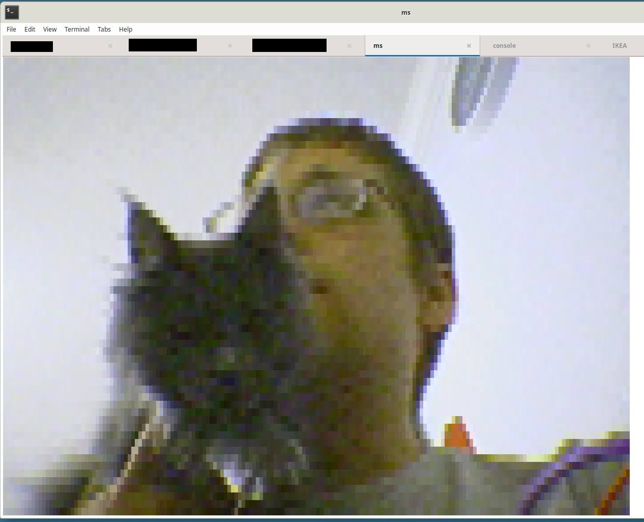
The MSIO camera is a very rudimentary camera sporting two possible resolutions: 176x144 and 352x288. It provides data in YUV422. It supports some basic settings and effects. White balance is configurable between the settings of: auto, incadescent, flourescent, and outdoors. Exposure is configured in 8 steps. An effect may be applied, one of: black and white, sepia, negative, and solarize. The camera supports live preview in the 176x144 resolution. Here you can see a sample low-resolution photo. A lot of documentation that follows talks about delays. They are NOT optional and skipping them will cause issues.
The layered protocol
The camera protocol seems to be layered in a very strange way. A command-reply interface is fashioned out the MSIO register read, MSIO register write, and MSIO interrupt requests. A command is composed of three bytes, and it may have up to 8 bytes of parameters and may return up to 8 bytes of reply. First, a packet is composed, made of: {numReplyBytes + 1, numParamBytes + 4, cmdByte0, cmdByte1, cmdByte2, params...}. This packet is always 13 bytes, with unused parameter bytes being random garbage. The strange additions to length are not that strange. Byte at index 1 is simply the number of bytes in the command (including itself). Byte at index zero is the number of bytes expected in the reply, including the reply's own length byte. More on that later.
The command is written to registers 0x25..0x31. A 300-micro second delay is observed now. Then, using a second register write operation, register 0x32 is written with a value of 0x10. This tells the stick to execute the command. You must now wait for the stick to signal interrupt. Then wait 800 microseconds. Then using a register write operation, register 0x32 is written with a value of 0x01. This tells the stick to prepare its reply in the reply registers. Again, you wait for interrupt, and then 500 microseconds. Now the reply may be read starting from register 0x33. Precisely "numReplyBytes + 1" bytes shall be read. Compare the first byte read with "numReplyBytes". It is an error if these values are not equal. Congratulations, you've completed one mid-level MSIO camera command.
On top of this mid-level command interface, another layer is built. It allows reads and writes into indirect high-level registers of arbitrary lengths. These registers are addressed using two bytes ADR0 and ADR1. To read a high-level indirect register with address ADR0;ADR1, issue a mid-level command with the command bytes 0x01, ADR0, ADR1. Command parameters are a single byte - the length of the high-level indirect register being read. Command reply is the register value. To write a high-level indirect register with address ADR0;ADR1, issue a mid-level command with the command bytes 0x02, ADR0, ADR1. Command parameters are the bytes to write to the register. Command reply is an echo of those bytes. A mismatch is an error.
Curiously no other mid-level commands are ever observed in the existing driver.
The init sequence
After the function is enabled, a delay of one second must be observed. After this, this high-level indirect register 1;1 must be writen with the bytes 0x00, 0x62, 0x02, 0x06. Now a delay of 75 milliseconds is needed. Then the camera resolution must be set (more on this later). It can be changed later, but it must be set to one of the two values here. Next, the 1-byte-long high level indirect register 2;4 is read. In the read value, bit 1 is cleared, bits 2 and 6 are set, the value is then written back. Next, a few more high level indirect registers are written with one byte values as follows 0x73 -> 2;29, 0x93 -> 2;30, 0xC4 -> 3;11, 0x23 -> 3;12. The camera is now initialized.
Next the camera settings are set. They can also be changed at any time, but they must be set to valid values here. By default, the effects are disabled, white balance is set to auto, and exposure is set to 5. At this point photos may be taken, resolution may be changed, and settings may be reconfigured.
Setting settings
Each setting is represented by a one-byte high level indirect register.
The photo effect is represented by the register 1;5 and it is a bitfield! Bit 4 removes color information. By itself it creates the "black and white" effect. Bit 5 adds yellow. Together with bit 4 this will create a "sepia" effect. Bit 6 inverts the image. Bit 7 is responsible for the "solarize" effect which will basically sharply raise contrast and darken overexposed pixels. These can be combined at will. The lower 4 bits do not seem to do anything.
White balance is a value between 0 and 7, inclusive that is stored in the high level indirect register 2;5. The known values are 0 for "auto", 1 for "incadescent", 5 for "flourescent", and 7 for "outdoors". Other values are also some settings but I do not know the names as the driver app makes no use of them.
Exposure is a value 1 thorugh 8, inclusive that is stored in the high level indirect register 4;7
Setting resolution
To do this we'll need to read the normal MSIO reg 0x23, and the high level indirect register 1;4. If we'd like to use the high-resolution mode we now clear bit 5 in the value read from MSIO reg 0x23 and clear bit 2 in the value from 1;4. For low resolution mode, we set those bits instead. We then write them back to their place: first the MSIO reg 0x23 and then 1;4. We are not done yet. The indirect reg need to be "accepted." To check for that we read it and wait for the value we read to match what we had written. The value is now properly set. The same read-and-wait method can be used with the settings described above. If this is not done, you might find half a photo frame affected by the new setting, and half by the old. Always fun.
Taking a photo
To take a photo, just start reading it. Read using READ_LONG_DATA TPC in 0x200 byte chunks. The first read might take up to 600ms. This time will be inside the handshaking MSIO procedure, so prepare accordingly. The card does not use MSIO interrupts so the only way to get the data to flow is to busy wait in the handshaking stage. After the first chunk is read, the subsequent chunks do not incur this delay and are readable instantly. A low resolution image is 50688 bytes, which is exactly 99 READ_LONG_DATA TPCs. A high-resolution image is 202752 bytes, which is 396 READ_LONG_DATA TPCs. You must read the entire image with no interruption. If you do not, the camera will (1) not produce new images and (2) resume reading from where you left off if you try to read again. There is no way that I know of to fix this other than a power cycle.
The data format is YUV422. Note that u and v are sent as unsigned and need 128 subtracted from them to be the proper expected signed values.
The Chip
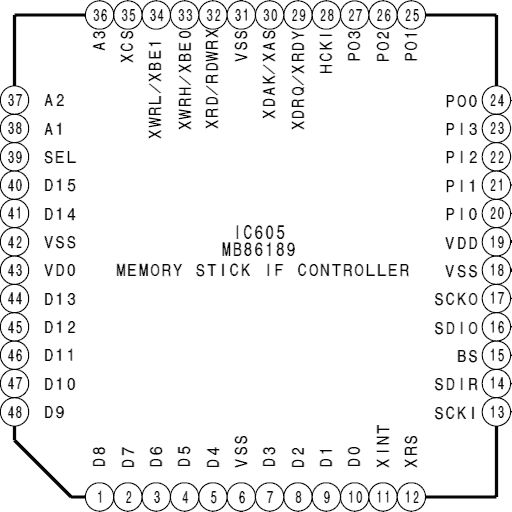
Many devices that supported Memory Stick did not use SoCs that had Memory Stick Host IP - they used a separate chip. In fact, many of the earlier Sony devices also did that. The chip is always the same - MB86189. Thanks to Sony's own Service Manuals we even know its part number (8-759-584-32) and pinout. That is great, but not nearly enough info to sort out how it works. There is work to be done here too. But first let's inspect the pinout. Clearly the interface is 16-bit parallel. There are 3 address lines, which means, barring some weird indirection, at most 8 internal registers. There are byte lane selects (XWRL, XWRH) to allow byte writes (not just word writes). The chip can output interrupt signal. There is a DRQ line, so the chip probably supports DMA of some sort. And finally, it clearly does not support the parallel Memory Stick interface.
I started reverse engineering Sony PDA's drivers in the devices that had this chip. It did not take long to figure out some basics and produce my own driver to talk to it that worked. I then tried to produce a working driver for another device that used a MC68SZ328 chip, which has built-in Memory Stick Host IP and does not use this chip. What struck me is that MC68SZ328's Memory Stick Host IP almost perfectly matched my reverse-engineered MB86189 registers. I dug deeper. I found a few other SoCs that have Memory Stick Host IP built in, like the iMX1 ARM SoC. They ALL had the same register set and bits! It really looks like Sony only developed this IP once, and then sold it to everyone, and also incorporated it into MB86189.
There were a few differences. The IP in all the SoCs has two general purpose inputs and two general purpose outputs. Their bit positions in the register that controls them would have them be #4 and #5. MB86189 has four of each, and their bit positions are 0..3 in MSPPCD register. Also all the registers except MSCS and MSRDATA/MSTDATA are now byte-accessible. They are also byteswapped compared to the datasheets of the Memory Stick IP in all those SoCs I just mentioned, if accessed as words. So, to use MB86189, just refer to the iMX1 manual. I did not verify if auto-command mode works as it is not very useful. This will now allow proper emulation of this chip and proper use of it, if you so wish. Here is the register layout:
Later, opening an Acer s65 I discovered another memory chip to interface to Memory Stick. It was a W86L387D. Curiously, the pinout and driver both matched Sony's MB86198 chip! Who knows, maybe they are related?
Code for download
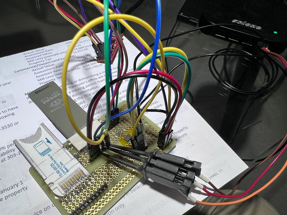
Provided code is in a few parts. First part is a very very basic implementation of the low level 1-bit-wide protocol bit-banged on an STM32 chip. With cleverness you could use the SPI unit, but on purpose that is avoided to make this more widely applicable to other microcontrollers. Optimization is left as an exercise for the reader. This code will print attributes of a Memory Stick Pro and try to read and write some sectors. For a memory stick classic it'll find and display the boot block. Code is "hacky" quality at best. :)
The second piece of code is a simple implementation of a Memory Stick Classic flash translation layer.
In the "more" directory is some code showing use of the memory stick camera and memory stick gps.
License is: free for noncommerial use. For commercial use (haha) contact me.
Comments...
