Repurposing boring eInk electronic shelf labels / price tags into useful photo frames / status displays, with blackjack and hookers custom firmware and greyscale! Quick video (partially sped up) here: [LINK]. There you can see association, image download with progress bar, and image display in greyscale + yellow.
UPDATE 1: Added details on Chroma29, ZBD devices
Table of Contents
- eInk price tags basics
- Let's Begin
- Digging Deeper
- We Need to Talk...
- Librarification
- eInk
- My Tag Firmware
- The Other Side
- The Wireless Bits
- Another tag!
- That Large, Three-colour Panel
- Another: PriceData Chroma29
- More Yet: ZBD devices
- More SoluM devices
- Downloads & Use
- Comments...
eInk price tags basics
What they are and what they are for
They have been appearing in stores since the early 2000s, but have really become prevalent in the last five to seven years! Also known as ESL (Electronic Shelf Labels), they basically allow the store to change prices dynamically as they see fit, without having to send a person out with a new printed piece of paper to place unto the shelf. The extra benefits include ability to show off more of the product's features (bullet point lists often shown on large price tags), change that shown feature list (advertise differently based on current day/month/etc), and use colours (last five years brought red and yellows to the previously only-black-and-white electronic shelf labels). There is a lot more marketing fluff about why ESLs are cool, and you can read all about it on your own time!
Common features
Most of the current-generation ESLs are updated wirelessly, using some sort of a custom protocol. The company "Pricer" distinguishes themselves here, using InfraRed instead, making their devices completely useless for us. InfraRed is dead, guys, get over it! Anyways, all of the protocols are of cource not documented, so we're on our own.
Most of the current-generation ESLs use eInk displays (aka: EPD - electrophoretic displays). Why? The main selling point is power. eInk uses none while it is showing a static image. You've likely seen a screen of this type last you looked at an eBook reader, like a Kindle. They do need power to change their contents (quite a lot actually), and are a giant pain in the rear to work with in general, but more on that later. Having a screen that needs no power to show prices, combined with the fact that prices do not change often, leads to good battery lives. Multiple years is the advertised figure. Based on my work below, I believe it entirely, and I was even able to improve on it!
Let's Begin
How I got involved
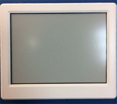
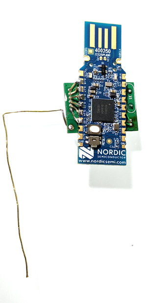
I saw some "Samsung NFC Tag ST-GM42KC0 Solum ESL SmartTAG" listings on eBay. I figured that I was, at the moment, short precisely one interesting project, and given that is was an electronic device, there was approximately a 100% chance I'd be able to bend it to my will. I thought it would be a cool way to show weather and stocks in an easily glanceable fashion in the morning. Maybe a cool black-and-white picture frame too? The listing said these were NFC based, but the model number I looked up at the FCC website showed that this model lacked NFC. Fine, NFC is no use to me anyways. Clearly they are not updated in the store over NFC (what good is an electronic price tag if you need to send a real live human to update it?), there must be some real wireless in there somewhere. I clicked "buy", and waited.
Let's look inside

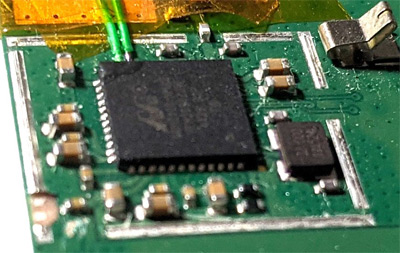
Well, that is not that exciting, some passives, two 2.4GHz antennas, and a shield can. No fun at all! Where's the beef? The board is attached to black plastic by super-strong double-sided tape. The screen is attached to this same plastic from the other side using the same kind of tape. Of course the eInk panel is also by a company that no longer exists and no documentation exists either... Time to open it up!
After prying the annoying metal can off the board, I could finally see the brains of this operation, and my heart sank. "Marvell" No name elicits such a visceral response as that one. These are the assholes who bought Intel's X-Scale SoC line, deleted the datasheets off the website, and then found every datasheet copy on the internet and had it taken down. If you ever have a choice between working with their chips and paying twice the price for some other chip, pay someone else twice as much, thank me later. They have a pre-arranged, reserved parking garage just for them in hell! The chances of ever seeing a real datashet were now clearly zero. Damn!
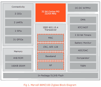
Well, in any case, predictably googling for 88MZ100 produces nothing but Marvell's own website, with their public "datasheet" for the chip. Wait, didn't I just say they do not have datasheets? Yeah, they indeed publish a PDF for each chip that they call "datasheet". It serves as a giant "screw you" to all developers who would futilely hope that it would contain specifications of how the chip works or how to use it. This one was two pages long. The only useful thing it contained was a diagram roughly outlining the features of the chip. Well, ok, now we know that it is a Cortex-M3 (most any chip made this decade would be), it has 512K of flash, 160K of RAM, and speaks ZigBee.
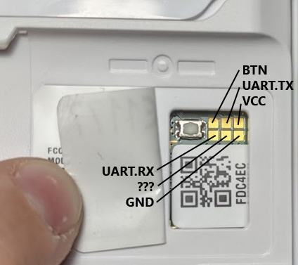
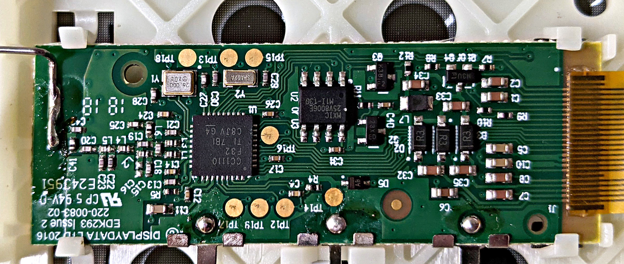
The board also had a 2x3 arrangement of landing pads for pogo pins, clearly for factory programming/testing. This is obvious since they are accessible from the outside, hidden behind the serial number sticker on the back of the device. Scoping them as the tag was powered up revealed that one was power, one was ground, and one was a TX line of a UART, configured as 115,200 8n1
Cortex-M class chips are debugged using a standard interface called SWD that was designed by ARM specifically for this purpose. This is nice compared to the 10000 different interfaces that are used to program/debug 8-bit microcontrollers. Conveniently, I have a wonderful SWD debugger called CortexProg that I can use. SWD uses just two pins, one for clock and one for bidirectional data. I tried those 6 pogo pin landing positions in every possible order, and had no luck. Hmm, well on every chip I've ever used, the pins for these two were next to each other. Obviously nothing requires that, but it is common. I decided to try my luck and try every pair of nearby pins to see if I got any response to my SWD debugger. Well, what do you know? I get a response from the chip when I use pin 22 as SWDCK and pin 23 as SWDIO.
Show me the code!
Most production devices lock the chips in a way that their code cannot be read out. This protection is usually a big deal, and is often advertised for chips. It is strange that Marvell did not advertise anything of the sort. Could it be? Does this chip really lack something as basic as an ability to prevent code readout? Well, as far as I knew at this point, perhaps. Plus, Marvell is not exactly known for competence (just for being assholes), so I would not put it past them to forget something this obvious. In any case, I tried to read it using CortexProg. It worked... It reads 128K of ROM. Yes 128K, despite the "datasheet" saying 4K. Well, what did you expect? It is Marvell. Not only that, I could also debug the code successfully. Step, set breakpoints, everything!
The chip, however, seemed to crash often when debugged. A bit of sleuthing revealed that it was being reset by the watchdog timer. Now, most Cortex-M chips are designed by intelligent people, who realize that debugging needs to happen, so they either design the WDT to pause while debugging is ongoing, or have a bit somewhere to configure that, and default to pause while debugging. But of course, Marvell...
The flash seemed divided into four parts: a bootloader, some binary data that later turned out to be radio calibration and settings, what seemed to be peripheral drivers, and what looked like a complete ZigBee stack. How did I know? ZigBee packet format is rather specific and code that parses it has a rather obvious shape. And I've seen enough i2c and spi drivers in my life to recognize one by code shape quite easily. But randomly stopping the device while it was running revealed that it ran from RAM, never entering ROM. This one fact tells us three distinct things. One: the peripheral drivers and ZigBee stack in the ROM are unused, Two: The code in RAM must thus have its own comms layer. And three: that code must be coming from somewhere, and it is not in the ROM!
Digging Deeper
Where is the rest of the code stored?
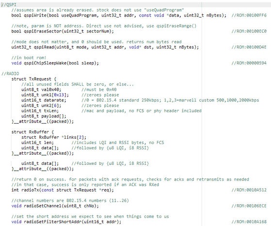
Remember that block diagram? "In-Package 512KB Flash" it said. But how is it addressed? To figure it out, I'd have to disassemble the bootloader. Luckily, it was only 4KB in size, and did not call out to any other code - fully self-contained. If the bytes 0xAB, 0x06, and 0xB9 mean anything to you, you'll immediately realize, as I did, that the internal flash must be attached over an internal SPI bus. Those are typical (de facto standard) SPI/QSPI NOR flash memory commands. Knowing that, in turn, allowed me to label the functions and sort out more or less how the SPI peripheral works in this SoC. It also showed where the code comes from, and what the bootloader does. It seems like the internal interface is actually QSPI.
So, what does the bootloader do?
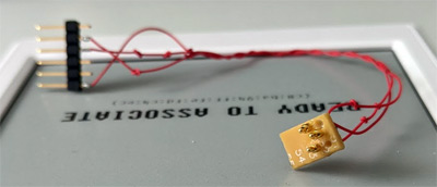
The bootloader starts by reading the first 32 bytes of the QSPI flash into RAM. It is checked for a magic number, and if it is not found, the bootloader enters a loop looking for a UART that it can use (it tries all possible pinmuxes of all UARTs for receiving a magic char with a small wait on each possibility). If the magic number is found, a few words of those 32 bytes are used to configure both UARTs. Then another is used to decide if SWD will be ok. I guess this is their way of locking out code readout - by locking out debugging. A poor strategy, that is easily glitched. Oh well, it's Marvell... Then comes a checksum of the "application" and a few bits to indicate its type ("none" is an option, and this device uses it), and then the QSPI address of the "application", its size, the RAM address to load it to and its entry point address. A word contains a password, defaulting to 0xffffffff, and Samsung/SoluM uses that too, luckily. Another config word defines how long to give an external user to interrupt the boot process by sending a magic character over a UART. If the checksum matches (or none is used), and said timeout has passed with no magic characters RXed on the UART, the application is loaded into RAM and control passes to it. Else, the device goes to an interactive UART shell. Here you can see the pinout of the debug connector and the pogo-pin jig I made to interface with the devices, so that I could talk to the bootloader's command shell.
The interactive shell protocol was not hard to decipher, and I wrote a tool to talk it. It is in the downloads package on the bottom of this page. The protocol is a rather simple command-response deal, of the type anyone would implement if given the task. There exist two commands to read and write memory directly (MMIO, RAM, ROM), commands to read the QSPI chip or directly send it a given command, a command to reset the chip, a command to enable/disable SWD, and a command to jump to a given address. Note that this does not include QSPI write/erase. While the bootloader has code for that, no possible command reaches it. Luckily, the "jump to given address" command can be used to jump to it directly. It works. It should also be noted that the commands have a password system. Luckily our tag does not use it. Else we'd need to provide/guess a given 32-bit password.
Now, you would think that we're lucky that no password was set by Samsung/SoluM, but actually, it would not stop us at all. After 256 wrong password attempts, the chip will erase the QSPI memory and reset. And as you remember from above, when QSPI is erased, SWD is enabled, and the password for commands is 0xffffffff, once again allowing us in just fine. Since QSPI is erased sequentially, 4KB at a time, a simple power interruption after the 256th wrong password would allow us to happily read out most of the flash. Marvell...
The REAL firmware
Now that I had a convenient tool to talk to the bootloader, dumping the QSPI, and thus the REAL firmware was a matter of one simple command. It was large, and had a lot of complicated control flows. It had 49KB of code, 1.5K of various initialized data, and even a [0-9A-F] subset of a 16x16 font. A quick analysis showed a few interesting things. First was the confirmation that this code makes absolutely no calls to the ROM drivers or the ROM ZigBee stack. I saw this earlier from stopping the chip with the debugger, but now it was confirmed - this application code is entirely self-contained. The second thing I noticed is that this code also did not contain a ZigBee stack of its own. Searching for code that looked that it parses ZigBee packets did point me in a few directions, but all of them seemed too simplistic for real 802.15.4. Strange...
The UART is live even after the application boots. And I saw that it claimed to be scanning for a base station, and then eventually it gives up. Looking at the code that, by now, I was sure parsed the incoming packets, I was able to deduce what packet it would expect such that it would go down the path that shows the message that it found a potential master to associate with. The packet parsing was weird, though. ZigBee is built on 802.15.4, which defines the lower layers. It has 4 basic packet types: BEACON, COMMAND, DATA, and ACK. Assuming I was reading this assembly correctly, this code dropped all packets that were not of DATA type. This is strange, but code does not lie. It was time to talk to it, but how?
We Need to Talk...
Let's send some packets!
Both the "datasheet" and the antennas on the board make it clear that this chip works on the 2.4GHz frequency band. In that 2.4GHz band, 802.15.4 prescribes using QPSK modulation at 250Kbps, with a 5MHz channel spacing. The QPSK part is difficult. Most cheap radio chips support ASK/OOK, FSK and GFSK. QPSK support is uncommon. Looking around my lab, picking up random radio-capable things, and checking for what they support, I quickly arrived at the nRF52840 Dongle. It, allegedly supports ZigBee, and thus must be capable of this modulation. A quick read of the documentation revealed that it is. It took a day or so to put together some code to squirt packets of the proper format out into the air, and ... nothing.
Luckily, Nordic also provides firmware for their dongle to be used as a ZigBee sniffer. I loaded that up on another dongle, and started listening for my packets. Nothing. It took a bit of debugging, but I finally figured out that I had misread a sentence in the nRF52840 doc. After making a fix, the sniffer saw my packets. Sending them very rapidly and turning the tag on did indeed produce a message from the tag that it found my "base station" at an RSSI of -50. Sweet. It was time to analyze the protocol, but then I saw something that immediately cooled my enthusiasm. The stock code that speaks to the display forced it into a 1bpp use - black and white, no greyscales! No good!
A sad plot twist
It is approximately at this point in time that some idle searching on my favourite chinese stolen-documents-and-sources-site showed that while there are no results for "88MZ100", there was one for "MZ100". Do my eyes deceive me? A real datasheet, 704 pages of it! It is, of course, watermarked with the name of the company it was given to, and all that. Exciting, right? Of course not, it is Marvell... There is no data on radio, QSPI, clock unit, or power management unit. All the information in this datasheet I had already figured out by reverse engineering. It was useless!
Librarification
Custom Firmware on an Undocumented Chip?
Once it became clear that I'd need to write my own firmware for the chip, my main worry became the radio. Sure, I can figure out timers, memory, QSPI, and all that, but I'll never successfully fully reverse engineer an unknown radio peripheral, and make it work as well as the people who have the docs. Radios are complex, require complicated calibration, power management, and settings. Reverse engineering a radio is possible, but not likely, and not fast. Definitely not a fun project. It is just too complex to do quickly, and I am too easily bored to do it slowly. Additionally, power management is also another one of those things that is hard to do without the docs. Another approach was needed!
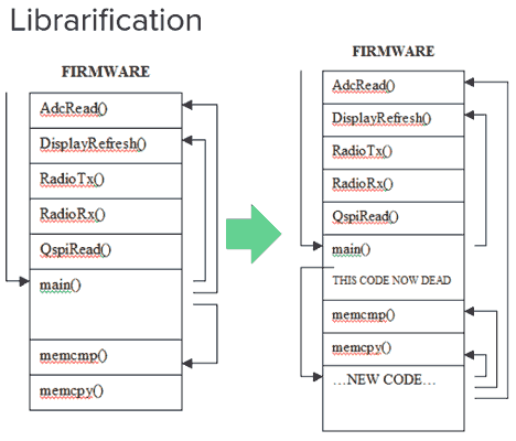
I am not sure that Librarification is a real word, but this is the word I created to explain this method of hacking up existing code. I've used it before for patching complex drivers on unfamiliar systems to add only a few extra functionalities. The idea is simple: First append some more code after the existing code. Use some linker script magic to tell the linker where existing useful functions are, and make an include file to tell the compiler about them. Same for global data. Now, just find a logical place in the main function after most of the initialization is done, and place a jump to *your* main function. Thanks to compiler and linker scripts, you'll now have access to the whole old existing firmware as a library!
Size matters!
The one issue with librarification is size! Due to how the 88MZ100 bootloader loads code, and the choices Samsung/SoluM made with their memory layout, the total code size was limited to 0xF000 bytes. This left me with about 6KB of space for my code. Luckily many utility funcs I'd need, including things like printf, strcpy, and memcmp are available for the use in the stock ROM! I did run out of space eventually, though. I looked and found some more code in the stock ROM that was now unused so i was able to subsume that space as well - another 4KB or so. So now my code was appended to the stock ROM, AND embedded in it. Sadly GNU Linker simply cannot cope with a discontinuous code segment in an automated fashion, so I was forced to manually allocate functions to this new space. I just moved two of the largest ones. Easy!
eInk
The theory
This is a short, over-simplified, not-quite-accurate explanation of how eInk works. First, let's talk about normal garden-variety black-and-white eInk screens. They are a sandwich of special goop between two pieces of glass - front and rear. Like on an active-matrix LCD, the rear glass has transistors on it per-pixel. This allows one to apply specific voltages to each pixel in the display as needed. The goop in between the pieces of glass is rather interesting. It is some sort of viscous transparent oily substance, the composition of which is a closely-guarded trade secret known only to the eInk corporation, and the million-or-so chinese companies making knock-offs. In this goop, float two types of particles. Their specific chemical compositions are, of course, a big secret as well. However, the big picture here is clear. The particles that are white are also statically positively charged. The particles that are black are statically negatively charged. Now it is obvious how it works. If you apply a negative charge to the electrode on the bottom of a pixel, white particles will be attracted down to the electrode on the bottom, and black particles will be repelled to the top (towards the glass the user sees). Bam! Black pixel. Do the reverse and you get a white one. Easy so far. Makes you wonder what is so hard about this whole eInk thing.
The practice
As always, the real world is not as nice as the theory would imply. The oil that the particles are suspended in, of course, gets more viscous the colder it is, as all liquids do. This means that it takes more force (or more time) to move the particles through it. Also, if it is not shaken up for a while, it also gets more viscous (like honey). This means that when you want to change a pixel, not only does the temperature and its current state matter, but also it matters how long it's been since you last changed it. But wait, there's more! Long term imbalance in applied charge can damage the particles. Basically, if you already drove the particles up, and you apply more force, repeatedly, you can permanently damage them. This looks a lot like OLED burn-in: a permanent ghost image superimposed on the actual image you are trying to show. Now you are beginning to see that driving eInk is not so simple afterall. And this is just for black and white...
So, how do you get grey colours? Well, by driving some white and some black particles to the top! How? by quickly alternating applied voltages, and relying a bit on inertia. As you can imagine, here precision is even more important. For simple black-and-white, if you push white particles up a bit too much, you still get perfectly serviceable white, if you push black particles too much, you still get a reasonable black. However, without very precise control, your greys will be inconsistent, or even nonexistent (blending with white or black).
Partial screen update (fast update) is even harder since you need to know the current state perfectly, which you do not - there is no per-pixel measuring device of any sort. This is why even fancy eInk screens and fancy drivers (like kindle) show some ghosting when they do partial updates a few times in a row. The solution is a full update (also known as "flashing update" or "slow update"). It resets all pixels to known states and removes ghosting.
LUTs/waveforms
Who would better know how to drive a screen than a manufacturer? Nobody. So, of course, manufacturers provide these waveforms (usually termed LUTs) to customers. They are considered a trade secret and are basically unobtainium. Even chinese clone makers do not give theirs out unless you buy a few thousand screens. Some give out "sample waveforms" that sort-of work at a given temperature for black and white. Nobody is giving out good greyscale waveforms! All of these price tags never needed greyscale, so despite their screens being perfectly capable of greyscale, this capability was never used.
The screen controller matters too. Indeed you could slowly stack up waveform by hand, but it would get tiresome, so instead the screen controller has a few loadable waveform memories. The idea is that you can give it pixel values, and for each pixel it would do the proper waveform based on the pixel value. The controller in these Samsung/SoluM tags supports 4 shades, so it has 4 per-pixel-value LUTs that you can load, and the image data uploaded to it is 2 bits per pixel. The practical upshot of this is that with proper waveforms, getting 4 greys out of it is just a matter of uploading image data. Getting more greys would requite multiple uploads and multiple different waveforms.
Guess-and-Check x1000
Sadly, I had no grey waveforms at all. The stock firmware just had waveforms for black and white, as it never used any other colours. This being my first foray into eInk, it took me more than a week to sort out what each byte in the waveform bytestream means, and how to tweak them properly. In the end, however, I did produce a working set of waveforms that can do a full update at room temperature to get four greys. As I plan to use these indoors, temperature ranges outside of room temp do not worry me, but I did test my waveforms between 10 and 30 degrees C and they work well. I did not, initially worry about partial updates, but later I did implement basic partial updates so that I could show a progress bar for loading next image. Partial updates are almost impossible to do in greyscale without manufacturer help, so my progress bar is purely black and white (but it does not disturb the existing greyscale image, just takes up the top two pixel rows. A full screen update with my greyscale waveforms takes about 4 seconds on this display.
While looking at how stock firmware works, I noticed a bug in their code that loads waveforms. I think they copied the code from their same-type price tags that support black/white/red screen type. Those use more LUTs. The current code loads 8 LUTs, but the grey screen only has 5, so they load 5, and then overwrite the first three with random garbage from memory. Due to the memory layout, this means that they are using the wrong LUTs for every temperature range, and for highest temps, using garbage entirely. So much for testing :)
My Tag Firmware
Use cases
My wishes were simple - a wire-free picture frame that can be updated remotely. I designed the firmware and protocol around this. First, I designed a storage system for settings that wear-levels across some large amount of flash, so as to not kill flash prematurely (it has a limited number of write cycles, you know). Then, I designed a simple (but extensible) protocol for the tags to talk to the base station (which is still an nRF52840 dongle). The protocol also looks like 802.15.4 since that is what the Marvell radio supports/expects/can filter addresses on.
Basically, a tag, on boot, checks if it is paired to a master yet. If no, it goes to the pairing flow, else it goes to the check-in flow.
The pairing flow involves sending a broadcast packet at a very low TX power (so that only nearby masters hear it) advertising its capabilities and waiting for a reply. This is tried a few times on each channel. If no reply is ever received, the device goes to sleep forever to save power. The batteries can be removed and reinserted to try pairing again. If it does get a reply from a master, with a sufficiently strong signal level, it will consider itself paired. The master will provision it some settings, which will be saved, and the device will go to the check-in flow.
The check-in flow is simple. The device contacts the master on the proper channel and reports its battery life, OS version, and a few other things, like current temperature and the RSSI of the last packet received from the master. The master will reply with the latest version of image and firmware it has for this device and device type, respectively. The device will compare these versions to the versions in flash. If a firmware update on the master is newer than the current firmware, it will be downloaded and applied. If an image is newer on the master than locally, it will be downloaded and shown.
Downloading
Actual downloading is interesting, since it requires transfers of large amounts of data using small packets over an unreliable medium that is radio. Retrying too much wastes power. Retrying too little wastes power. Oh, and when it goes to sleep, 88MZ100 loses all RAM contents and reboots when it wakes, so we need to store all persistent state in flash. I designed a storage mechanism in flash to accommodate all of this. The Settings framework takes care of this. Images are downloaded a small piece at a time (64 bytes) and some flash is used to keep track of how far we've gotten. If the image is updated on the master, it will stop serving our requests for the old version, and we'll re-check in, realize a newer version exists, and start downloading that one instead. More on all of this later.
Security
As we all know, the #1 priority of the CIA, KGB, and the chinese secret services it to intercept my wireless photo frame updates! I decided to fight back. All data sent between the master and the tags is encrypted with AES in CCM mode. The tags are pre-provisioned (in firmware) with a key that is used to encrypt the initial association request broadcast, and the master's response. The master's response includes a new key that is unique to that connection and will be saved by the tag in its settings. Nonce reuse is avoided by storing the counter that is the nonce in setting as well. Why such over-engineered security system for a photo frame? Why not?
Power
Power optimization is important. I noticed in the stock firmware a certain func called before some units were used, passed something that looked like a unit number. A similar func was called after some units were shut down. Having seen my fair share of embedded firmware disassemblys, it was clear that the reg these functions touch is the "power up" or "power down" reg. The bits in it were set to power things down. Well, I went and experimented to see what each bit powered down. The logic is simple. Set a bit, try writing/reading a reg in each peripheral that I know retains a written value normally. If it stops retaining, we probably powered off the peripheral. Luckily, unlike some other architectures, in ARM, given the large 32-bit address space, peripherals each get a generous chunk of it, so where any peripheral starts is generally not hard to guess. After some investigation, I was able to power off a bunch of peripherals and save a few hundred uA at runtime - every little bit counts!
While optimizing for power, I noticed that after I've called some radio functions, power consumption rose by a few mA and never fell back down. This would not do! After I finish with the radio comms, there is often other things to do before going to sleep, and there is no reason to draw a few extra mA during that time. Problem is, I have no docs on the radio, I do have the firmware though. Sadly the stock firmware never did anything about this (confirmed by measurement). But clearly if there is a way to turn something on, there must be a way to turn it off, right? I traced the calls with the debugger to see which bit of which reg being written causes the consumption to go up. I found a few. Sadly clearing them back did nothing. Must be one of those "write 1 for action, zero writes ignored" regs. What to do? I decided on brute force. I literally did this: memset(RADIO_PERIPH_BASE, 0, 0x8000). What could go wrong? Actually, power went down a little. Not all the way down, but a little. Then it was just a matter of binary search to find which bit in which reg did the work. Binary search is fast - I found it. What next? Well, clearly, memset(RADIO_PERIPH_BASE, 0xFF, 0x8000). Yup, that dropped some power too. Binary searching this found another bit in another reg. Clearing the former and setting the latter brought the board back down to the power consumption I saw before I ever touched the radio! Sweet! Curiously, the stock firmware never writes these bits.
To prevent tags stepping on each other repeatedly on the radio, the sleep duration is always randomized +/- 6%.
A Hardware Erratum
After a few weeks of use I noticed an issue: devices would sometimes hang, and drain the entire battery. Why?! I spent some time debugging it, and noted an issue: after the device was meant to go to low power mode, approx 1.5% of the time it would instead hang consuming 15 mA. I realized that this might be a hardware issue. Out of curiosity, i tried to see if the watchdog timer could help this issue. I set it up for a long delay and waited till the hang happened. Indeed after a few seconds, the device reset. So it looks like the watchdog works even when the chip is hard hung, not running any code. This might explain why the stock firmware had the watchdog on. I suspect this is a hardware erratum. In any case, keeping the watchdog on prevents the issue.
The Settings Framework
As flash memory wears out with use, storing settings in the same exact space would cause issues rather quickly, especially given that we'll need to write them almost every time we go to sleep, since nothing else persists across sleep. The solution is simple wear-levelling. Write newer versions after older versions, when we fill a whole flash erase-block, erase it and rewrite. Doing this across a few blocks is even better as we are at no point in time left with no valid settings, if we were to be interrupted. This does pose an interesting challenge. If a firmware update were to change the layout of settings, how would it handle reading old settings, should a power interruption corrupt the newer-format settings it may have written. The solution is not very hard. We include, in the settings header, a version and a size. The size field allows us to skip settings in storage (to go read the next record) no matter if we know what they contain. The version field allows us to update setting we read to the current version that we understand. Thus, if we read settings, and find settings v1, we can upgrade them to v2, then v3, and then v4. We can then write that back, marked as v4. This works since all new fields are always added at the end. Cool.
Image Compression
A simple backreferencing compression is implemented in my firmware. It saves 20% or so on transfer size. This was relevant earlier in development, when I still did not have radio working as well as it does now. This is not that useful now, but it remains, since it does save power. The decompression is very low-CPU use so no power issues there. Support for it is signalled in the association packet.
Picture frame mode
A little later, I realized that besides showing the image that was just uploaded, it might be nice to upload a few and have the tag auto-swap them. This is picture-frame mode. It is configured in the firmware and represents itself as a different device type over the radio. More on this later
Firmare update
As the device is on battery, and code space is limited, I did not spend effort and time to make updates brickless (unable to brick the device). As such, if you pull out the battery at just the right time diring the firmware update, you'll leave the device in such a state as to need recovery from a PC using a serial cable. I am losing no sleep over this. I do not expect firmware updates to be often, and for my use cases this is not an issue. It could be done, in theory, though.
Bardcode
Code128 is a barcode format that is very easy to generate programatically. I added ability to generate those to my firmware. On all UI screens, for example the "ready to pair" screen, a barcode encoding the MAC address is shown. This is especially useful on devices with a vertical portrait-mode screen where the whole mac does not fit within one screen width.
The Other Side
Station Hardware
The station hardware is pictured here: nRF52840 and a ti cc1101 board with a custom antenna. The blue LED on the nRF52840 dongle blinks whenever we send a radio packet - a nice way to know things are working. You'll see it light up solid when an image update is being sent to a tag, as many packets are exchanged rapid-fire. The TI radio board is for the second tag type I support - more on that later.
Station Firmware
So what does the master's firmware look like? I wanted to make it as simple to use as possible. The nRF52840 dongle acts like a USB stick, formatted with FAT12, with 960KB of storage, more or less. All current operating systems do not cache writes to external media because it could be ejected anytime. We use this! The firmware in the master reads the FAT and the root directory when it wishes, and has the same view as the host computer's OS. The firmware never writes there. So what does it look for? When a tag with the MAC address GG:HH:II:JJ:KK:LL:MM:NN checks in, the firmware will look for a file called LLMMNN.IMG. If found, it will be offered for the tag to download. But, above, I mentioned that the tag decides to download an image or not based on version. Yes. The "version" here is a linear combination of "creation date" and "modified date" such that if either rises, the version will increment. Very very simple and efficient.
Firmware updates are handled a bit differently. They are handled by "device hardware type" which is a field in the check-in packet. The idea is simple: if you have a new firmware - it should apply to all devices of the same type, no need to discrimiate based on MAC address. These Samsung/SoluM black-and-white tags are allocated a hardware type of 1 and thus their updates would be downloaded if they are named UPDT0001.BIN. How does versioning work here? Per hardware type, the firmware knows at what offset in the update the version is stored. This is done to avoid re-downloading older firmware by accident, if the file was touched somehow. This all works!
An annoying question arises: the master must now keep track of all of these per-device encryption keys, which is a nightmare. Furthermore, as the master does not have infinite storage space, this limits the number of tags a single master can support. This will not do! The solution is simple. The keys can be made such that the master can re-derive them as needed. How? The master can start with a single "root key" derived from some chip-unique material. Then each tag's key is simply AES(root_key, salt1 || tag_mac || salt2). Now, as long as the root key is not known to an adversary, we've accomplished both secure comms and using zero bytes per-tag on the master's side. Cool!
Image format
The image format I picked was simply BMP format. The stock firmware did this, and I did not see why not. I found out soon enough. BMP supports one bit per pixel, 4, 8, and so on. Some old WindowsCE versions supported 2-bits-per-pixel bitmaps, but no other existing tools do. Nothing supports 3 bits-per-pixel bitmaps. However, the format itself easily lends itself to these things, and I decided to use the format still. I wrote a tool bmp2grays that can ingest a 24-bits-per-pixel true-colour bitmap, and convert it to a given bits-per-pixel bitmap, optionally with dithering. The tool supports 1,2,3,and 4 bpp, with an optional non-grey colour (red or yellow, more about this later). This tool's source is also part of the downloadable package at the end of this article. The firmware on the tag will accept any depth bitmap and downsample/upsample as needed for the tag, but obviously uploading a proper-bit-depth image is best
The Wireless Bits
Protocol
The protocol was designed for low power on the side of the price tag. Keeping a radio receiving costs power, quite a lot actually. So the tag cannot just always be in receive mode. Some protocols solve the problem with timing. You pre-arrange when the device will wake up and listen on the radio - Bluetooth LE does this, for example. This requires a precise clock - that in turn costs power too. Luckily not much - most modern chips can keep a 32KHz oscillator running for a low low cost of a few microamps. But, why bother with that? I decided to not even pay this cost. The base station will be powered, so it can always receive.
When a tag is erased, or newly flashed, it begins by attempting to associate with a master. It does so by sending out a broadcast association request at a very low transmit power on every channel, in turn. The request contains tag information, like hardware type, battery level, and screen size/type/resolution. The master who receives this request may choose to accept it. If the tag gets a positive and valid response of at least a given signal strength, it will accept it. The signal strength limits make it just a bit harder to pair with someone else's tags. The thresholds chosen require the tag to be basically right on top of the base station to pair successfully. As both sides check for signal strength, being evil and pretending to be close would be difficult without a very very large transmitter. The pairing response packet contains some configuration data for the tag. Some info is also assumed, for example the channel number where the response was received is saved and from then on used to communciate with the master. The most important thing in the response itself is the parameter telling the tag how often to check in. This will literally determine how often the tag will wake up and report back to the master. Setting this high improves battery life, as sleep may last longer. Setting this low improves responsiveness, since no image uploads may happen until the tag checks in. For once-daily updated tags I chose 1 hour check-in period. This parameter, however, is configured in the station firmware and is up to you to change as you see fit. A couple of other check-in-related parameters are supplied at association time. They are: the number of failed check-ins needed to blank the screen and the number of failed check-ins needed to disassociate from this master. Either or both can be zero to disable such functionality. The idea is simple. If you do not update the tag images often, how will you know that they are still communicating properly? Well, you could check the base station's logs, but I wanted a more visible notification. If the "number of failed check-ins needed to blank the screen" setting is used, and that number of check-ins in a row fail, the screen will change to a "TOO LONG WITHOUT CHECK IN" message. It will revert back to the last image if a checkin succeeds. The second parameter is a convenience. As these tags lack any sort of convenient user input, I wanted at least some way to erase them to pair them to a new master. This is how! After this many failed check-ins, the tag will erase all association info and go back to its unpaired state, ready to pair again. The association response packet also contains the encryption key the master has provisioned. It is saved and will be used from then on to secure communications.
The normal flow, when paired, is simple. When the tag wakes up from sleep, it will prepare a check-in packet. This contains the current battery level, the received signal strength and "quality" estimate from the last packet it had gotten from the master, and its hardware and software versions. This is sent to the master, and if no reply arrives, four more attempts are made, after a few hundred milliseconds. The check-in response packet tells us what versions (if any) are available on the master for us of IMAGE and FIRMWARE. If either is higher than the versions we have locally, we perform a DOWNLOAD. If both are available, FIRMWARE takes priority.
The DOWNLOAD process is simple. The tag requests a piece of a given version of IMAGE or FIRMWARE at a given offset. The master will send back that piece, or an empty packet if that version is not available. This handles the case of a yet-newer version becoming available mid-download. That will cause the DOWNLOAD to restart. Each piece we receive, we write to flash, and then clear a bit locally in a flash manifest area to record we have it. This allows the process to resume no matter how and when it was interrupted. If a request to download a chunk is not replied to, a retry is made. After a few retries, we give up and go to sleep. We'll retry later. How much later? If at least a single piece was successfully downloaded this session, one second later. If not, at next checkin. This provides for automatic handling of collisions and temporarily-bad RF environments. Once a download is completed, we act on it. In case of IMAGE, it is drawn. In case of FIRMWARE, it is applied immediately, and a reboot is performed into it.
Frequencies/channels
802.15.4 uses the same spectrum as WiFi/Bluetooth/microwaves/etc... Needless to say, frequency selection is crucial. At my house, zigbee channel 20 was the most free, so I used that one. About 99% of packets make it across the house error free. By comparison, channel 11 only allows 80% of packets to pass through. Station's channel is configured in the station firmware.
Future-proofing
The protocol has a version field, provided at association time, so that the base station knows what "language" the tags speak. And all the packets have a few bytes reserved and required to be zero for now. This allows for very easy extensibility in the future, by simply reusing these bytes to mean something. This is safe as we know that any old firmware will set them to zero and will not read them. Extensibility for the win!
Another tag!
Chroma 74
At about this time, just as I decided the project was wrapping up, I saw some larger e-Ink price tags on eBay and bought them. These were the 7.4-inch DisplayData Chroma 74 devices. These were tri-colour e-Ink devices: Black/White/Yellow with a resolution of 640x384. They were also large and I was looking forward to making larger picture frames out of them, but plenty of new challenges loomed.
Let's open'em up!
Opening the device revealed a few things right away. First of all, the panel was soldered unto the board. No connector here - that is bad news. Means there is no simple way to reuse the panel. We must make peace with the existing board somehow! The main chip here is TI cc1110. The good news is that it is completely and totally documented. TI docs are usually very good, and this chip's docs are no exception. The bad news is that it is an 8051 - an architecture specifically created to make life hard for programmers. I'll get back to this later. Some of remaining interesting parts of the board are the two crystals: 32KHz clock crystal and a 26MHz crystal as required by the cc1110. The last interesting thing is the SPI memory chip - a Macronix MX25V8006E. It is a 1 megabyte chip. The size makes sense for the screen resolution.
It does...nothing
When powered up, the device does nothing. This is much less nice than what the Samsung/SoluM device did. We cannot sniff the screen initialization sequence if it is not done... This approach was not going to work...
The code
Connecting a CC-DEBUGGER (which I happened to have around) to see if I could reprogram the chip revealed a pleasant surprise - the chip was not code locked and the code could be read out! Well, this makes life easier. I could probably make sense of what it does and go from there. I had never worked with an 8051 before, but I figured it is just another chip, how bad could it be?
8051
In 1980, the 8051 might have been a nice microcontroller. It has plenty of amenities and functionality that would have made it a fine choice for any design back then. Sadly, some silicon manufacturers have not gotten the memo that it is more than 4 decades later. For today's world the 8051 is a mess. Nowadays serious firmware is programmed in C, not in assembly, and 8051 is uniquely unsuited to be a target of a normal C compiler. For starters, it has at least 8 possibly-overlapping types of memory, each with its own limitations and abilities: 4 banks of 8 8-bit registers, which are also mapped to RAM, 128 bytes of RAM, accessible directly via instructions or indirectly via R0 & R1 pointer regs; 128 bytes of SFRs, accessible directly via instructions; 128 more bytes of RAM, accessible indirectly via R0 & R1 pointer regs; 128 bits that are individually addressable using instructions, 256 bytes of external memory accessible indirectly via R0 & R1 pointer regs; up to 64K of external RAM accessible using then long DPTR pointer reg; and up to 64K of code memory, where code resides, also readable using the long DPTR register. The stack is limited to internal memory (256 bytes), and shares that memory with the registers and the bit-addressable memory. There is no notification of stack overflow either. Stick THAT into your compiler's pipe and smoke it!
Clearly, this is not a good place to build a compiler on. There are a few commercial offerings that actually do a passable job of compiling C to this hellish target, but even they need a lot of handholding (eg: programmer manually assigns which memory to store variables in). Compared to hand-rolled assembly, I'd score these compilers' output at about 1/10th as good, and 1/10th as compact. They are also quite expensive. There is also an open-source free compiler called SDCC. Its only benefits are that it is free and standards-compliant. The code generation is atrocious, to say the least. But, it is free. In the interest of others' ability to reproduce my results, I decided to target SDCC. As every version of SDCC works differently, and my code bumps against many limits, you'll probably want to know that my code was built with SDCC version 4.0.7, which I built from source. I know for sure that my code will not build with 4.0.12 - it will claim to be out of memory. YMMV.
Due to the very tight memory limitations in a few memory types, about 80% of the effort involved in writing C code for 8051 is randomly rearranging code in functions and randomly retagging variables to different memory types to see if this solved the dreaded cannot find 7 bytes for DSEG or Unable to find 4 free bytes in PSEG error messages. Since the stack is very small, parameter passing through the stack is not advisable in most cases, so it is done via globals. Sadly, this means that the more functions you have, the more RAM is permanently allocated to their param passing locations. Ideally those could be overlaid on top of each other, but in reality it almost never works out due to various limitations of SDCC. Both of the expensive compilers (and, I think, SDCC too) have a mode where they by-hand synthesize a software stack in external memory. This is slow and code-heavy but solves a lot of other problems. I did not choose to go that route due to the speed penalty involved.
All of the large memory areas (code memory and external RAM) are accessed using a single DPTR register, represented at two 8-bit halves: DPL and DPH. Since there is only one of these registers, most code that accesses multiple things in external memory, like, for example, memcpy or memcmp might, will necessarily spend about 95% of its time shuffling things back and forth in and out of DPL and DPH. Some 8051 derivatives, in fact, add a second DPTR register to make this easier, and add some way to switch which one is used. In fact, TI cc1110 DOES this too. Sadly, SDCC has no support for this. Using it manually in assembly would also not work due to how TI implemented this. It would break all interrupt code that SDCC generates that would not be aware that currently DPTR represents DPH1:DPL1 and not DPH0:DPL0. I decided to live with this limit, and never used the second DPTR. I am told this is common for many 8051 projects.
Reverse engineering 8051 code is also quite a chore. A processor that does so little per instruction necessarily mandates using complex instruction sequences to do what should be simple. In the interest of saving code space, these sorts of things end up functions with weird calling conventions and weird purposes. For example, implementing switch() in 8051 is commonly done with a function call, followed by some format of a jumptable. The Chroma 74 firmware uses two separate such implementations - one for dense cases and one for not. I wrote some IDA scripts to process these and make them readable: 8051_switch_with_ranges.idc and 8051_dense_byte_switch.idc. They are part of the downloads package on the bottom of this page.
It should have been simple
I tried to port my Samsung/SoluM firmware to port to this tag. A lot of work was required to make it work though. Porting code from a 64MHz modern 32-bit chip with 160KB of RAM to a 26MHz museum piece with 4KB of RAM was bound to hurt.
Throughout my odyssey of writing the replacement firmware for the Chroma 74 device, I kept bumping into various limits. At some point in time it became clear that I had to rewrite some code in assembly, so I got into the habit of randomly looking at the generated assembly so that I would know where the most egregiously-bad code was. I'd then target that for hand-written-assembly treatment. Over time, I implemented most of 64-bit math: u64_copy, u64_isLessThan, u64_isEqual, u64_add, u64_sub, u64_inc, u64_dec. This had to be done because otherwise SDCC insisted on permanently allocating 8 bytes of the valuable directly-addressable internal memory for temporaries for any 64-bit operation. My functions operate only on 64-bit values in external RAM and take pointers to them, wasting no internal memory. I then implemented much better variants of memset, memcmp, memcpy, and strlen as well, optimized for size and speed. At one point in time I even implemented, in assembly, the full xorshift128p random number generator, but I did not end up using it.
I then noticed that SDCC particularly sucks at division and multiplication. This is actually an annoyance in the C standard, which says that when variables of type X are multiplied, the result is also if type X. This is very inconvenient, since multiplying two variables of length X bits produces a result of length (X * 2) bits. So if you want the 64-bit result of multiplying two 32-bvit values, it is not uncommon, in C, to do this: uint32_t a = ..., b = ...; uint64_t ret = (uint64_t)a * (uint64_t)b; Most good C compilers recognize this, and properly emit a single multiplication, storing the final result properly. SDCC does not. It insists on expanding both params to the final size, and doing the naive multiplication. It does this for any variable size. So, yes, I get it, the code says to do that, but that is NOT what the code means! Plus, with their approach, they take a lot longer to multiply though all those zeroes created by the extension to the longest type. To avoid this nonsense, I implemented and used my own functions for multiplication, in various sizes: 8 x 8 -> 16, 16 x 8 -> 32, 16 x 16 -> 32, and 32 x 8 -> 32. SDCCs division code was also pretty bad, so I wrote some replacement routines for a few sizes I needed: 16 / 8 -> 16, 32 / 8 -> 32, 32 / 16 -> 32, and 32 % 16 -> 16.
The final thing I rewrote, and the hardest was string formatting. This is the backend to printf/sprintf. Given that this project was my first time working with 8051, this part was particularly hard. I ended up working very hard to reduce RAM and CPU use here. I also learned about the double-dabble algorithm, as it needs less temporary storage than repeated division when printing very large base-10 numbers. My printf has some special 8051-specific optimizations. For example, instead of passing entire 64-bit values on the stack, if I want to print them, the * modifier in the format means that instead a pointer to the value in external RAM is provided. Such a pointer is only 2 bytes in size - a 6 bytes savings. A few other optimizations exist as well. See printf.c for all the gory details.
Serial Peripherals
The cc1110 has two serial ports, usable either as SPI or as a UART. Each of the functions has two sets of pins it can be assigned to. One port is allocated to the eInk panel, the other is wired to the SPI memory. However, the alternative mappings of the second port point to two test points on the board - a possibility for a debug serial port - a feature of great convenience. The port would have to be time-multiplixed between the SPI EEPROM and debug UART. Switching between them without glitching either turned out to be hard, and I was almost ready to give up when I stumbled upon the proper order of GPIO function switching and port pin mapping changes that caused no glitches on either port! Sweet! Now I could log to a serial console and use SPI EEPROM at thre same time!
I also wanted the potential to upgrade the device to a larger memory chip, so that it could store more photos in photo frame mode. This led to an implementation of SFDP. This is a specification of how an SPI flash can be automatically identified. My implementation is limited due to my needs and code size restrictions, but it will properly identify all flashes up to 32MByte and properly learn what size of erase operations they support and what commands that requires. I later upgraded a few of the tags to IS25LP128 - a 16MByte chip.
Test points
Some of the test points on the board are of interest. First of all, the TI debug interface. The nRESET signal is available on TP2 and TP12. The P2_1/DBG_DAT signal is available on TP3 and TP13. The P2_2/DBG_CLK signal is available on TP5 and TP15. VCC signal is available on TP4 and TP14. GND signal is available on TP8 and TP18. The pins I use for debugging are also available as test points. The P0_1 signal is available on TP6 and TP16. The P1_6 signal is available on TP7 and TP17. The P1_7 signal is available on TP9 and TP19. You may notice a pattern. Each signal is available on both sides of the board, with the test point names matching, just different by exactly ten.
Another Wireless Interface
This tag had a radio incapable of QPSK at 2.4GHz, so a new radio layer was needed. I decided to reuse the same protocol, just on another frequency and with another modulation. I went with the 915MHz band, and made sure the bandwidth was wide enough (more than 500KHz) to legally permit for any transmit power I wanted. GFSK modulation is used and 250Kbps is the selected data rate. I implemented a TI cc1101 driver in the firmware of the base station, and wired "radio index" through all the code in the station to support multiple radios. It took only a day, and it works beautifully! Actually wiring the second radio to the nRF52840 stick was quite easy - the photo earlier in this article shows how it looks and the source code for the base station has the wiring connections in tiRadio.c
Sleep
Curiously, the cc1110 uses less power in sleep than the 88MZ100. It also retains RAM while it does this (all but 350 bytes, for some reason). However, reinitializing everything after sleep is a bit of a pain, and uses even more code space, so instead I just reset on wake. This is the same thing that 88MZ100 does and my code already was built around.
That Large, Three-colour Panel
Three colours are harder than two
Same as before, this explanation is very oversimplified to as to be short. You have been warned.
Predictably, this was also my first time working with a three-colour eInk display. I sat down and started to do more reading to try to figure out how those are driven. These usually come in Black/White/Red (BWR) and Black/White/Yellow(BWY) colour choices. Strangely there is no blue option. Problem is, there are only two types of charges: positive and negative. And we already had two colours for particles: white and black. So how do we add another colour, without iventing new types of physics? Turns out that there is no way. Instead, yellow particles are also negatively charged, just like black, but, they are smaller and thus more nimble. The driving chip also gains new abilities: two new voltage levels, lower than the previous ones we had used for driving black and white particles. For example, this display uses +/- 5V as the low driving voltage, and +/- 20V for the high driving voltage.
So how does it work? Actually not very easy at all. White colour is still easy, since white is the only positively charged particle type still. Black and yellow disambiguation is much harder. If we apply a positive charge, black and yellow both are drawn to it, and we get what looks more or less black (as black overpowers yellow). To make yellow appear, we apply short bursts of negative high voltage to drive away both yellow and black a little while not completely drawing white to the top, and then we apply a long burst of low voltage positive charge, to attract just yellow. Doing this a few times allows us to develop Yellow+Black into just Yellow. Easy.
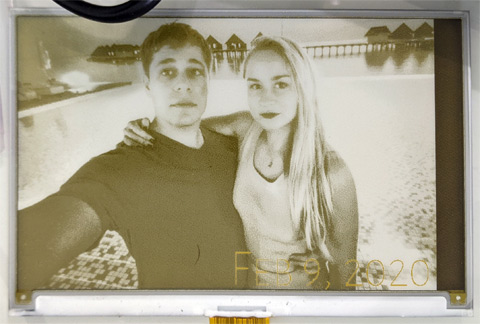
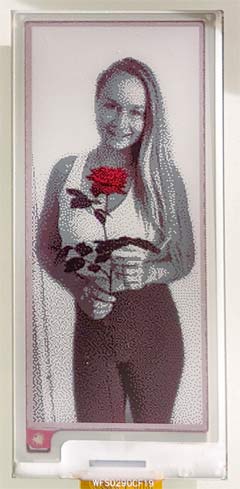
Greyscale
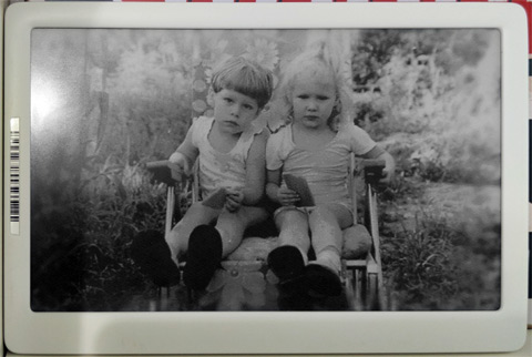
Getting three colours out of a three-colour eInk panel is not hard, as I figured out rather quickly. Getting working greyscale turned out to be very very hard. The problem is that using low voltage does not move black particles very much as they are larger. Using high voltage moves yellows as well, so all greys end up poisoned by yellow. This gives photos a rather strong sepia effect. The first photo on the right shows what that looked like. Cute, but not what I wanted. It took a few weeks of experimentation to figure out how to get better greys. The solution was all about timing the pulses. In the simple black-and-white screens, two short pulses had almost the same effect as one longer pulse. In the Black/White/Yellow screen, this is no longer the case. We can also take advantage of inertia. If we start the yellow particles moving AWAY from the screen, we can give a short pulse to move blacks up to the top, and hope that the inertia of the yellows moving down keeps them from moving up too much. Repeat a few times, and you can get relatively good yellow-free greys. It all sounds nice and easy as I explain it, but it took a long time for me to figure this all out. The second photo on the right shows what it looks like now - perfect achromatic greys. A full screen update with these waveforms takes about 52 seconds, which is pretty good for the picture quality obtained! Partial update for just black and white mode takes half a second. This i used for the download progress bar that shows up on top of the screen at download time.
Having accomplished perfect greys, I went on to produce waveforms for a number of shades between black and yellow, and then some for the white-to-yellow range. Those were actually quite easy since they just require simple high-voltage pulses from fully developed yellow colour. But this was too many colours. The controller in this screen supports 3 bits per pixel, so without undue annoyances, 8 colours are possible to have onscreen at once. I decided that a splash of yellow is nice to have, but I mostly care about more grey shades for better reproduction of greyscale photos. So the colour selection I went for was: 7 shades of grey from black to white at indices 0 through 6, and one bright yellow colour at index 7.
Another: PriceData Chroma29
So very similar
Chroma29 is a small (2.9inch) tag from the same family as the Chroma74. These also come in BWR and BWY variants. I had a few of the red kind so that is what I tested on. The wiring is the same as the Chroma74. The EEPROM, however, is smaller. The firmware is actually almost the same as the Chroma74 as well, except the display driver. The display resolution is 128x296 at a pixel density of about 110dpi.
Making more out of less
The controller only supports 3 colours: Black, White, and Red. Unlike the Chroma74 controller, it really only has 3 LUTs (meaning it can only create 3 colours onscreen at a time) and, as a further cost reducing measure, it lacks the ability to generate the low magnitude negative voltage. Why? Well, you'll recall from earlier: to show Yellow (and Red) we just apply a low positive voltage to drive the Yellow/Read particles up. We use a high positive voltage to get black, and a high negative gets us white. Indeed in a display intending to show just those three colours, there is no use for low magnitude negative voltage. My issue is: I do want to display greys. As you'll recall from above, to display greys unpolluted by the third colour, we DO need the low negative voltage. However, what use is the ability to show greys if we can only have 3 colours onscreen at a time due to the controller only have space in its internal memory for three waveform tables? Curiously, the solutions to these two problems dovetail nicely.
Recall that the way I got nice greys on the Chroma74 was to start with a white, and then run a few cycles of repelling yellow and then attracting black. Well we'll do the same here. But we only have three waveforms we can use at once. And we have no way to repel red as we lack a low level negative voltage. So let's take it in steps. First, we'll create the black, white and red that we need onscreen, where we intend to use grey, let's make white for now. Easy enough, this screen controller easily handles that. Now we'll obseerve that voltages on the controller are controllable. We can adjust just how low the "high magnituge negative" is. Officially it goes down to -6V, but if we extrapolate the values in the table in the datasheet, we can get it down to -4.5V, where we want it. Measuring the capacitor onboard confirmes that this works. Ok, that solves the low magnitude negative issue, assuming we do not need high magnitude negative anymore. Now what? Well, we ARE limited to two greys here, but that is better than none. We have three waveform tables. We'll use table #0 for "light grey" and load the proper waveform in there to drive away red and attract a little black. We'll use table #1 for "dark grey" and load the proper waveform for that there, and table #2 will be "keep", which will be loaded with all zeroes. So now for all light and dark grey pixels we send the proper index, and for all black, white, and red pixels we send index 2. So yes, we need to load entirely different data into the display RAM buffer now, but so what? We do and... it works! So we did it in two phases, cool.
There is a bit more to do here, however. The repeated oscillations of the grey waveforms will slightly corrupt the edges of nearby red/black/white pixels, so we need to re-firm them. This is almost simple. Red, Black, and White are 3 colours total, so we need to do this in two phases as well, since we also need to allocate a waveform to "keep" to leave the greys alone. So, for phase 3, we load up waveforms for "black", "red", and "keep", send data to the screen to point out the black and red pixels, assigning greys and white to "keep". We then do a 4th phase, where we re-firm white the same way. Does it work? Yes it does. We get wonderful greys out of this process, producing a 5-colour display. Much better than simply Black, Red, and White! The software support for all of this multi-phase stuff took the form of #define SCREEN_DATA_PASSES 8 in screen.h declaring how many times the screen driver needs to be given the image data. This is necessary since we lack the RAM to buffer the whole image. We instead decode it as we read it from the EEPROM a few times. Why 4 and not 8? This controller needs to be fed black data first and then red data. It does not accept them in an interleaved format as Chroma74 screen did. This is actually the more common form, and Chroma74 is the outlier
An astute reader might ask if this can be extended further, adding two more levels of grey per phase. The answer is no. Greys themselves are very sensitive to nearby colours, so trying to create some more greys while keeping some existing ones will cause the existing ones to distort.
Saving space
As each pixel can have one of 5 colours, using 3 bits per pixel seems like a bit of a waste. On the other hand, 8051 is a very weak CPU and trying to do fancy compression on it is unlikely to work. What can be done? Simple math to the rescue! If each pixel can be one of five colours, we can multiply the value of the first one by 25, the second by 5, and add in the third. This will allow recovering them using simple 8-bit division & modulus operations that 8051 can do. The maximum value from this kind of calculation is 124, just under 127 - the maximum value storeable in 7 bits. This means that on average each pixel uses 2.33 bits - 22% smaller than using 3 whole bits for each pixel. I added support for such packing in a generic form to the firmware. This particular scheme is called 3x5_7 for: "three pixels with a multiple of five, stashed into seven bits". I later also added 3x6_8 for 6-colour displays and 5x3_8 for simple BWR/BWY 3-colour images. The former is an 11% space savings, the latter saves 20%. The converting program has, of course, been updated with these abilitites too.
On the Chroma29 this compression actually helps a lot. As each EEPROM flash block is 4KB in size, and images must start and end on block boundaries, without the compression, each image needs 4 blocks, but with 3x5_7, images fit into three. As Chroma29 only has 64KB of flash, of which 32KB is reserved for OTA, and a few more KB for misc. purposes here and there, this allows more images to be stored - a significant win!
More Yet: ZBD devices
Before PriceData became PriceData they were called ZBD, and, among other things, they developed a very cool technology - persistent LCDs. That is: an LCD screen that takes no power to main its state, only takes power to change it. That property is similar to eInk, but with a worse contrast ratio, no greyscale possibility, but much faster update. Also, like any other LCD, if you remove the backing, the screen becomes transparent. This is kind of cool too. I got my hands on some of the old ZBD devices (some are still on eBay - search for epop900), and added support for them too!
EPOP50
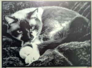
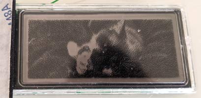
EPOP50 is the small (2.2inch display area) price tag, 51x21mm, with a resolution of 224x90 at 110dpi. Reverse egineering the comms protocol between the display and the processor was key. Since the display is custom and was never documented, there was no datasheet to find. In the end, it was pretty simple. The protocol is quite typical (SPI, top bit means "read", etc). I documented the commands in screenLCD.c. The only interesting thing is that the processor must measure the temperature and send that to the display for refresh to work properly. Otherwise, EPOP50 is wired precisely the same as Chroma device were, with no surprises of any sort. After all, this device is their direct predecessor. This display type cannot show greyscale in any way, as each pixel is bistable - can only be on or off. Combine this with low resolution, and you see that this device is not that exciting for picture frame purposes. Nonetheless, I added support for this device in my firmware. If you squint just right, you can see a picture of my cat here on the right.
EPOP900
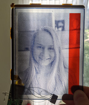
As far as I can tell, this is the original ZBD price tag. This device is so old, it predates them putting that nice SPI-based controller right into the screen. This display is driven with a lot of signals manually. This took a while to figure out since the firmware is also clearly older. Even the wiring is different from all other PriceData/ZBD devices. The display is 360x480 (portrait style) at 100dpi. If you peel off the backing silver sheet, it is transparent, which is kind of cool! They also integrated a red area into the screen - not into LCD itself, just between the layers. I guess this is used in retail to put the price there and have it stand out. It is just a piece of coloured film and is not controllable in any way. It is also not easy to remove, sadly. You can see what this looks like on the right.
Driving this display is much more complex than dealing with eInk screens or even their custom EPOP50 controller. 18 pins in total are used! Two are used as PWM outputs, with a capacitor and a resistor for smoothing to generate the two necessary voltages. These voltages differ based on ambient temperature. Eight pins are used to feed data, eight pixels at a time in parallel. The rest of the pins are various control signals: two are power enables, one toggles erase (this screen type needs to be erased before it is drawn), there is an enable pin, a pixel latch pin, a row advance pin, a row latch pin, and a frame marking pin. The code driving it in their firmware was unreasonably complex and used too many function pointers! Function pointers are a giant pain in the rear when trying to reverse-engineer 8051 code. You can see the gory detals in screenRaw.c. The practical upshot: it works!
On the right you can see one of these displays with the backing silver film removed showing off its transparency and the annoyingly unnecessary red stripe. I will, at some point in time in the future, try to get the stripe removed, because otherwise a transparent persistent LCD display is very cool!
My published firmware now supports this price tag type too
More SoluM devices
It all started with a SoluM device. But, it turns out that their second-generation electronic shelf labels no longer use a Marvell MZ100 chip. They now seem to use a custom chip of some sort. It is branded SEM9110 and has a SoluM logo on it. Searching online reveals that before the chip was branded SEM9110, it was branded ZBS242. More searching finds some more info about the chip (in Korean). From the look of it, Samsung took the MZ100, replaced the CPU core with an 8051 for cost savings, and fabbed it. It took a long time to reverse engineer the chip, and that is the subject of another article: Reverse Engineering an Unknown Microcontroller. I had two graphical tags based on this chip: both 2.9 inch. One was version 025, the other version 026. You can tell by powering them up. The number shown on top of the screen is the version. These devices all have 1MByte of EEPROM, which is nice and spacious, even if we allocate 64KB to OTA.
I used the code from my ZBS24x reverse engineering to build the code for the firmware. It took quite alot of refactoring to allow this firmware to be built for such differing chips. Some things had to be redone. For example my assembly-implemented printf had to be rewritten since in ZBS24x chips XRAM and CODE are in fact differing memory spaces, not the same as they are in TI's CC111x. A few other places in code assumed this equivalency and had to be corrected. Also, if ZBS24x has an AES accelerator - I do not know about it, so I had to implement AES-128 in assembly. It is not too slow - about 2ms per block. Random number generation also required some custom work since there is no hardware LFSR that I know of like the CC111x's. I implemented xorshift128p in assembly for that. Luckily ZBS24x has 64KB of flash so there is no shortage of code space!
Unlike CC111x this chip cannot execute code from RAM, so OTA was a bit more complex. What I decided to do was to write the whole updater in assembly, using only position-independent instructions (not all 8051 instructions are). Then, I copy it to the last page of internal flash (at address 0xfc00. Then I cna jump to it and have it update the rest of the firmware. This works well.
Then, I wrote the MAC address into the INFOPAGE in the chip, since stock firmware stored it in the main flash area, and that is not the place for it. I then noted that the INFOPAGE has calibration values for the temperature sensor. The chosen points are very strange (30 degrees C and 45 degrees C) but they work and the calculated temperature if very accurate. Sadly there is no way I found to measure the battery voltage, so I was forced to improvise. The display controllers have a "low voltage detect" feature with adjustable voltage levels. I use that. Sadly they only go up to 2.6V, but that is better than nothing.
These devices also have NFC built-in, in the form of an I2C-attached NT3H1101. I have not yet found a clever use for it, but I'll think of something. Talking to it does work so there are possibilities!
The wireless protocol used here is the same as I created for the original SoluM device: ZigBee-like packets on 2.4GHz.
Version 025
The display controller here, based on the command set I saw in the stock firmware, seemed to be the same as in Chroma29: the UC8151c. This made life easier since I already had code for it. Really this took very little coding to function. The same 5 colours as Chroma29 shows work here too in the same way. I even used basically the same LUTs
Version 026
It took a bit more investigation to figure out what he display controller used here was. After some comparison with various datasheets, I concluded that it was a SSD1675A, but with a few commands from SSD1675B. The LUT format that works is definitely SSD1675A's but some commands used in the stock firmware do not exist in SSD1675A but do in SSD1675B. This controller has four waveform slots in memory, which means that: (1) we can make it show 6 colours and (2) re-firming step can be done in only one phase instead of needing two. Both are true, and indeed it shows six colours properly. This tag uses 3x6_8 compression.
Support for these tags is now also part of my firmware. I considered adding support for the segment-display-based ones but as they do not show graphics, they aren't all that much use so I did not. Though simply for remote-mounted temperature displays it may still be worth it.
Downloads & Use
Overview
Well, here it it, what you came here for. The license is simple: This code/data/waveforms are free for use in hobby and other non-commercial products. For commercial use, contact me. The downloads include the source code for my firmware for the Samsung/SoluM 4.2 inch black and white tags, the source code for the bmp2grays program, the source code for my custom firmware for the Chroma/ZBD device, and the source code for the base station to allow all of them to be used and updated. I am also including binaries, in case are too lazy to build the code yourself. [DOWNLOAD HERE]. Update (jul 2022): here is newer 8051 code that also has a nicer build system. See Makefile for how to use. LINK.
Misc Notes
The uart tool for the Samsung/SoluM device has some special commands to ease converting them to my firmware format. makeDmitry command will flash a stock-firmware tag to my firmware, preserving its MAC address. updateDmitry will update a tag with my firmware, preserving its MAC address. Using any other method of writing to the tags will likely destroy the MAC address. This is not unrecoverable (it is stored at 0x74004 in stock firmware, 0x6c000 in mine), but annoying. My firmware will refuse to run without finding a valid MAC address. Stock will run but use a default one.
The downloads package includes all the binaries as well. Station/Station.bin is the firmware for the nRF52840 dongle. It will auto-detect whether a second radio is attached and should be used. This is not necessary for Samsung/SoluM device support, but is for Chroma/ZBD devices. This firmware expects to be flashed directly to the chip with no bootloader or such nonsense. It uses the entirety of the chip for storage of images, except the 16KB that it itself occupies. Chroma_fw/prebuilt has the firmware for the Chroma and ZBD devices, which you can flash using a CC-DEBUGGER or any other method you like (there are arduino scripts out there as well, I am told). solum_BW_4.2_fw/QSPI.bin is the firmware for the Samsung/SoluM 4.2 inch black and white device. You can flash it using the uart tool. If you choose to do it manually, remember that EEPROM writing does not auto-erase, you need to do that. I stongly suggest using the makeDmitry command instead.
The Chroma/ZBD firmware supports photo frame mode (auto-cycle) based on a compile-time define. Look at #define PICTURE_FRAME_FLIP_EVERY_N_CHECKINS in main.c. If you define it, you'll get a picture-frame mode firmware, and it will self-identify as device type: {3 for Chroma74, 5 for EPOP50, 7 for EPOP900, and 9 for Chroma29} on the radio. If you do not, it will only show the last thing sent to it (good for status displays) and will self-identify a device type: {2 for Chroma74, 4 for EPOP50, 6 for EPOP900, and 8 for Chroma29}. The differentiation is so that they can receive different firmware updates (and thus stay differentiated).
The released versions are: 1.1.0.0 for Chroma/ZBD firmware and 1.0.0.7 for the Samsung/SoluM firmware
Comments...
