Table of Contents
- A difficult start
- We can talk to it!
- Let's get to work!
- Fancier Features
- Radio
- Unsolved mysteries
- ZBS242/3 Pinouts, functions, SFRs, Downloads
- Lessons for aspiring reverse engineers
- Comments...
A difficult start
The story so far...
As part of my work on reverse-engineering eInk price tags I ran into an interesting problem. One particular company (Samsung Electro Mechanics/SoluM) switched from a third party chip I had figured out (Marvell 88MZ100) to a new chip in their next generation tags. This chip seemed to be made by them, custom, for this purpose. This never bodes well for reverse-engineering. A friend provided me with a few tags containing this chip to play with. There were two types that had a segment-based e-Ink display and one that had a normal graphical eInk display. They had the same main chip on them, so I started with the segment-based device, since it is easier to understand a simpler unknown system. It was not quite clear where to start, but, of course, that kind of puzzle is always the most interesting!
Research

It is stupid to try to solve a crossword puzzle without reading the questions. It is equally stupid to try to reverse engineer a device without first gathering all the info that exists about it already. So, what do we know right away? The wireless protocol is likely the same as before, since no company would want to try to migrate to a new one, or maintain two at once for customers doing a slow migration. The old protocol was ZigBee-like on 2.4GHz, so the new one likely is too. We also know what we can see. Here you can see the photo of both sides of the board (click to embiggen). So, what do we see? First, a very cool case of cost-optimization. They've laminated an e-Ink screen right onto a PCB! Who needs a conductive glass backplane when you have a PCB? The front is a piece of conductive plastic. But that is irrelevant. We see two antennas, both, given their size, for 2.4GHz. This was expected, since the previous generation devices also had two 2.4GHz antennas. We see two chips. One large one small. The large one (labeled "SEM9010") seems to have a lot of traces going to the display and none to the antennas. Clearly it is the display controller. The small one (labeled "SEM9110") seems to be the brain of the operation. It is connected to the antennas, to the timing crystal, and to the test points, which are clearly there for factory programming. There are 12 pads: one is connected to the battery's positive terminal, one to ground, the 10 others a mystery. Searching for the chip name online produces nothing of value - clearly it is a custom thing. But who designs a custom chip for something so simple? Maybe it is just a re-brand? We must try harder!
Curiously, Google image search helps here. It is an unexpected but very useful tool for reverse engineering sometimes. In this case, it leads us to this gem (archived here for posterity). It is a StackExchange question asking how these electronic price tags work. The reason it is interesting is that the PCB photo posted looks almost identical to ours. The chips look the same too, but they have different labels! This is probably from before SoluM started re-branding these chips.
The chip we had suspected to be the display controller is labeled SSD1623L2. This is indeed a segment e-Ink display controller, supporting up to 96 segments. Searching online finds us a pre-release version 0.1 datasheet (archived here for posterity). This is good! If we know how to speak to this, we might be able to identify the code that speaks to it, if we ever see the code, that is!
The main MCU is revealed to be one ZBS242. Well, OK. That is not a microcontroller I am familar with. Searching the internet some more finds us a link (archived here for posterity) that that StackExchange answer also mentioned. The page is in Korean, but it shows that this chip has an 8051 core, and a rather predictable set of peripherals: UART, SPI, I2C, ADC, DAC, Comparator, Temperature sensor, 5-channel PWM, 3-ch Triac controller, IR transmitter, Key scan functionality, RF-Wake, antenna diversity, and a ZigBiee compatible radio and MAC. The image shows that it also has 32KHz internal RC oscillator and claims to be able to consume just 1 uA in sleep mode. I guess this is the company that made the chip for Samsung. Interesting...
Some more searching shows that the die of our mystery SEM9110 has been imaged directly as well (archived here for posterity). The die claims to be a ZBS243. I guess that means there is a whole family of chips: ZBS24x. Interesting indeed.
We have a lead!
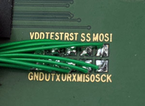
Opening another one of the segment tags provided some more good news: the programming header is labeled in clean readable golden letters! Looks like the header has SPI, UART, a reset pin, supply, ground, and a pin called "test", probably used to trigger factory test mode. Curiouser and curiouser.
Logically, the earliest member of a hypothetical ZBS24x family would have been "ZBS240". Maybe searching for that will lead to something intersting? Searching for "ZBS240" and filtering out the chaff leads to another interesting page in Korean (archived here for posterity). Looks like this company makes custom gang-programmers on demand. Browsing their website leads to a manual (archived here for posterity) for their programming device, and even a download of a PC-side utility to use it. The utility even has a firmware updater for the device. I took a look at it to see if I could glean from it how to program the device, but the firmware was encrypted. The PC-side utility seems to just send data to the device over a USB-serial port, so no good info in there either. Sad...
Some more searching leads to an even more interesting page (archived here for posterity). What is that? It is for sale?!? Certainly not anymore, right? Well, just in case, I did email the company. No reply... As a last hail-mary pass I asked a friend in Hong Kong if he knew anyone in Korea who might try to contact these guys, since their site does imply that they want a bank transfer from a Korean bank as payment. I myself did not believe my eyes when he got back to me and told me that, in fact, he can get me this device though a proxy in Korea! A few days later, it arrived by DHL!
We can talk to it!
How to communicate
It works! I can read and write to the chip! I took some time to explore the programming tool. The chip seems to have 64KB of flash and an extra 1KB of "information block" which, I guess, is used to store calibration values, MAC addresses, and the like. I captured some traces using the wonderful Saleae Logic of the programmer doing its thing. And you can download them here. You can see in that archive the traces for reading, erasing, and writing the INFOBLOCK and CODE spaces. The protocol is actually VERY simple! The clock speed can be anywhere between 100KHz to 8MHz.
The ISP protocol laid bare
It all starts with setting up the lines in the proper state: SCLK low, MOSI high, RESET high, SS high. This is held for 20ms. Next, RESET goes low for 32ms. Then, at least 4 clock cycles are sent on the SCK line at 500KHz. Then another delay of 10ms is observed, before RESET is taken high. There is now a 100ms delay before communications can be established. After this, any number of transactions may be performed. Some basic rules: there is a minimum of 5us between SS going down and a byte being sent, a minimum of 2us between the end of a byte and SS going up, and the minimum time SS can spend high is 2.5us. Each byte is sent thusly: SS low, byte sent in SPI mode 0, SS high. And, yes, SS toggles for each byte.
The transactions are all three or four bytes in length. The first byte is the transaction type, the lowest bit sets the transaction direction: a zero means write to the device, a one is a read from the device. Commands 0x02/0x03 are used to initiate communications. The programmer will send a three-byte write: 02 BA A5, and then it will do a read by first sending the read command and "address": 03 BA then the master sends FF while receiving A5. If this works, the communications are considered established.
Commands 0x12/0x13 are used to read/write SFRs into the CPU (I figured this out later, but it does not matter much here, actually). To select INFOBLOCK, SFR 0xD8 needs to be set to 0x80, to select the main flash area, it needs to be set to 0x00. To do the write of value vv to register rr, the SPI data is 12 rr vv. To confirm the value was written, it can be read back by first sending the read command and "address": 13 rr then the master sends FF while receiving vv.
Reading flash is easy. Command 0x09 is used for that. It is a four-byte command. After the command byte, the address is sent, first the high byte then the low. Then the master sends FF while receiving the byte that was read. Yup. You need a separate command for each byte read. Writing is also easy. Command 0x08 is used for that. It is a four-byte command. After the command byte, the address is sent, first the high byte then the low, then the byte to be written is sent. You need a separate command for each byte write too. Do not forget to erase before writing. Erasing is pretty easy too. Erasing the INFOBLOCK just requires a single 4-byte command: 48 00 00 00. Erasing the main flash is done using the command 88 00 00 00.
There, now with this info you can program your ZBS24x trivially!
Let's get to work!
| ADDR | x0 | x1 | x2 | x3 | x4 | x5 | x6 | x7 | x8 | x9 | xA | xB | xC | xD | xE | xF |
|---|---|---|---|---|---|---|---|---|---|---|---|---|---|---|---|---|
| 8x | P0 | SP | DPL | DPH | PCON | TCON | TMOD | TL0 | TL1 | TH0 | TH1 | |||||
| 9x | P1 | SCON | SBUF | |||||||||||||
| Ax | P2 | IEN0 | ||||||||||||||
| Bx | ||||||||||||||||
| Cx | ||||||||||||||||
| Dx | PSW | |||||||||||||||
| Ex | A | |||||||||||||||
| Fx | B |
A short primer on 8051
If you are already well-versed in 8051s feel free to skip this section.
8051 is an old intel-designed microcontroller from the dark ages. It is a gigantic pain in the ass to use, but it is still often used because it is cheap to license (free, in fact). So what makes it a pain? 8051 has a few separate memory spaces. CODE is the memory area where code lives. Its maximum size is 64KB (16-bit address). In most modern cases it is flash memory. Code can read bytes from here using a special movc ("MOVe from Code") instruction. XRAM is "external" memory. External to the core that is. It can be used to store things, but it is not much use for anything else. That is: the only operations one can do on this memory are read and write. Its maximum size is 64KB (16-bit address). How does an 8-bit microcontroller address memory with a 16-bit-wide address? Very slowly, it turns out. The movx ("MOVe to/from eXternal") instruction accesses this memory type, but how to provide the 16-bit address? A special register called DPTR ("Data PoinTeR") is used for this, and for the movc instruction instead. DPTR is made of a high register DPH and a low register DPL. Thus by writing half an address into each, external and code memory may be addressed. As you can imagine, this gets slow very quickly, since, for example, to do a memory copy from external memory to external memory would require a lot of shuffling values to and from DPL and DPH. Due to this, some fancier 8051 variants have multiple DPTR registers, but not all, and not all implemented the same way.
Intel did add a slightly-faster way to access a subset of the external memory. The idea here is to use R0 and R1 registers as pointer registers. But those are 8 bits in size, where will the other 8 bits of the address come from? They come from the P2 register (which also controls port 2 GPIO pins). Clearly this conflicts with using Port 2 for...well...GPIO. There are ways to mitigate this, but that is irrelevant. Memory accessed thus is limited to 256 bytes (unless you dynamically change Port 2, which you probably do not want to do). It is commonly referred to as PDATA. This kind of memory access is also done using a movx instruction. Next up, we have SFRs - various configuration registers that configure peripherals. This area is only accessible directly. That is: the address must be encoded in the instruction, no access via any sort of a pointer register. There are 128 bytes of SFRs. The table you see lists the SFRs available on a standard 8051. The grey-shaded cells are SFRs whose bits are individually accessible using bit-manipulation instructions. This is convenient to atomically set port pins or enable/disable interrupt sources or check some statusses.
The internal memory on 8051 is a bit complicated. On all modern 8051s there is 256 bytes of it. The last 128 bytes 0x80-0xff are only accessible indirectly via R0 and R1 registers, but unlike the external memory, we are no longer limited to only reading and writing. We can increment, decrement, add, and most other operations you'd expect. In fact ALL of internal RAM is accessible indirectly via those pointer registers. The lowest 128 bytes0x00-0x7f are also accessible directly (the address directly encoded in the instruction itself, same as SFRs. The 16 memory bytes in the range 0x20-0x2f are also bit-addressable using bit-manipulation instructions. This is a convenient place to store boolean variables. The lowest 32 bytes 0x00-0x1f make up 4 banks of registers R0...R7. The status register PSW has bits that select which bank is in use, but in reality since memory in internal memory area is usually tight, most code just uses one memory bank.
8051 is mostly a one-operand machine. That is: most operations use the accumuator as one of the sources and possibly a destination. The registers can be used by many operations too (but not all), and some operations allow indirect access to internal RAM, as described above. The stack is an empty ascending stack addressed by the SFR called sp and it lives in internal RAM only, limiting it to 256 bytes maximum, and a lot less in reality.
The start of any 8051 ROM image is the vector table containing jumps to the initial code to run as well as to the interrupt handlers. In 8051 tradition, the reset vector lives at 0x0000, and the interrupt handlers begin at address 0x0003 and continue every 8 bytes thence. Since the reti instruction is only used to return from interrupts, it can be used to easily find if some function is in fact an interrupt handler.
Stick all that into your C compiler's pipe and smoke it!
There does exist a passable C compiler for this architecture: C51 by Keil. But it is not cheap. There is an open source compiler too, SDCC. It sucks, but it is free. During this project I found only two show-stopping bugs that I had to work around in it, so not too bad for an OSS project.
Let's start the analysis
GPIO setup is easy to start with. Generally, you'll see a few matching bits being set or cleared in a few registers in a row. This makes sense, since generally you'll need to enable or disable using the pin as a function (versus GPIO), set it as input or output, and set or read its value. This sort of code would be expected pretty early on in the code. Let's see what we find... We find that the standard P0, P1, and P2 registers are indeed used in a way that would be consistent with being GPIO registers. By looking at what other registers are written around them, and whether bits in them are then read (input) or written (output) we can guess that registers AD, AE, AF are "function select" registers - GPIOs for which the corresponding bits are set do not seem to be used as gpios, and all GPIOs used as GPIOs are only so after the corresponding bit in one of these regs is cleared. I called them PxFUNC, where x is the port number. We can then conclude that registers B9, BA, BB control direction. Whenever a bit is set in one of them, the corresponding GPIO is only read, when the bit is cleared, the corresponding GPIO is only written. Thus we know that these regs control GPIO direction. I called them PxDIR, where x is the port number. Well, now I could in theory control GPIOs. If only I knew which ones did what...
I just decided to try them all until I find the one that controls the "TEST pad" on the programming header, or maybe the "URX" and "UTX" pads. Any really... I found that Port 1 pin 0 (P1.0) was "TEST", P0.6 was "UTX" and P0.7 was "URX". Having a GPIO we can control makes life easier, but there is only so long you can debug by toggling GPIOs till you get annoyed. It was time to improve on that!
We have printf!
I used this function to bit-bang a normal 8n1 serial port out the "TEST" pad, and used my logic analyzer to capture the output. I tweaked it till it was close enough to a baudrate that my USB-to-serial cable would accept! I already had an assembly implementation of printf for 8051. Within an hour I was able to output complex debug strings out this fake serial port. Not a bad start, and most definitely a requirement to proceed efficiently!
At this point I printed the values of all the SFRs to at least have a reference on what the values were. There were still some issues with exploring further. To start with, the watchdog timer (WDT) seemed to be on by default and would reset the chip after one second of execution, so all my experimentation had to be done in one second or less. I did not yet know how to control the WDT so I lived with the limitation for a bit. One second is a lot of cycles anyway!
Expanding our access
Now that I could reliably run code and print things, it was time to see where the clocking controls were. In almost all microcontrollers, there is at least one register that controls various speeds (at least CPU speed) and controls clocking (or reset) to various modules. The way to find them typically is thus: the former will usually be written VERY early at boot and rather rarely (if ever) touched again. The second will often have a bit set (clocking) or cleared (reset) before starting to configure a peripheral. We do not know where various peripherals are configured, but generally a set of closely-numbered SFRs correspond to a peripheral. So we look. There is definitely a register that matches this description, B7. We can see one bit at a time being set in it before some SFRs with similar numbers are written and bits in it being cleared after some similarly-numbered SFRs are no longer accessed. We can also see that initially it is written as 0x2F, so those are peripherals that are pre-enabled. Since bits seem to be set before what we assume are peripheral initializations, I'll call this register CLKEN. I played by changing the bits in this register and it seemed like clearing them did nothing. Kind of makes sense since I am not using any peripherals.
Another reg written near there (sane code usually initializes all of clocking together) and never written again was 8E. It is written to 0x21. I guessed that it might be speed related. I did some experiments. The bottom 4 bits seemed to have no effect, so I have no idea why they are being set to 0b0001, the next three bits, however, seemed to change the CPU speed quite seriously (as I could tell by the speed of my bit-banged UART). The top bit seemed to shift the frequency a bit, I suspected that it changed between internal RC and external crystal. The three bits I suspected to be a clock divisor set the clock speed, seemingly to 16MHz / (1 + value). I called this register CLKSPEED. Fastest speed is thus with the value 0x01, and the slowest is with 0xf1
Making timers work
Many vendors expand 8051s with all sorts of things, so there is very little standardization. However, most do not touch normal things 8051s have, like timer 0 and timer 1. Note, that this is a not a hard and fast rule. For example, TI does change timers significantly in their CC series chips. I noticed that in this chip, registers that would normally configure standard 8051 timers seem to be accessed near each other, and the interrupt handler #1 seems to touch them too. Could it be? Standard timers? I tried that and ... it worked. Completely standard as per the original spec, it seems. I checked the CLKEN register and found that bit 0 (mask 0x01) needs to be set for timers to work. I verified that the standard IEN0 register also works as expected and interrupt numbers 1 and 3 do indeed control interrupts for timer 0 and timer 1! The timers seem to tick at precisely 1/12th of 16MHz, same as you'd expect in a standard 8051 running at 16MHz. I have so far found no way to change this frequency. This knowledge now unlocks to us registers TL0, TH0, TL1, TH1, TMOD, TCON! We now have working precision timers!
I did check if the 8052(8051 sequel) standard timer 2 was implemented. It was not.
UART, maybe?
There were a few strings in the OTA module. Logically, they probably go somewhere, right? Maybe to a debug serial port? That would mesh together well with the board having "UTX" and "URX" test points. The code was a bit of a mess, but it seemed to stash bytes to some sort of a buffer. The code definitely looked like a standard circular buffer. I looked for where this buffer was read. It was in the handler for interrupt number #0. Ooh, interesting. Could this be the UART interrupt handler? The code seemed to check bit #1 in something that looked like a status register (reg 98), and if it was set, it would read a byte from our circular buffer and write it to register 99. If another bit (#0) was set in the abovementioned status register, it would read register 99 and stick the result into...yup...another circular buffer. Well, this sure as hell matches what I would expect a UART interrupt handler to be doing! How do we proceed?
Each circular buffer has two pointers: the read pointer and the write pointer. Logically, they should be inited before the buffer is ever used. So, if we find when those indices are initialized, we would likely find where the UART is set up, right? Sure looks so. In that function that initializes the UART, we see that GPIOs P0.6 and P0.7 are set to function mode, P0.7 is set to input, P0.6 - to output. Two more registers: 9A and 9B are written with 0x00 and 0x89 respectively. What I had guessed to be the status register (register 98) is written as 0x10, and then bits 0 and 1 in it are cleared. Then CLKEN bit 5 is set and IEN0 bit 0 is set. Well, this is basically all we need!
So, we name register 99 UARTBUF, register 98 becomes UARTSTA. We know that UARTSTA needs to be set to 0x10 to make the unit work, we know that its bit 0 means that UART has a free byte in its TX FIFO and that bit 1 means the UART has a byte for us in its RX FIFO. We know that CLKEN bit 5 enabled the clock to the UART and that interrupt number 0 is the UART interrupt handler. This is a goldmine of information. Given this, I was able to make a working UART driver in my code and was able to send a message out on the proper "UTX" pin, which we now knew to be Port 0 pin 6 (P0.6). We also learned that "URX" test point is wired to P0.7 and is the UART's RX line. The UART was sending data at 115,200bps, 8n1, and it was not affected by CLKSPEED register in any way. So what are those other two mystery registers that got those magic values?
I tried playing with those other two registers 9A and 9B. It quickly became clear what they are for. They are the baud rate divider registers. I tried a number of values to figure out how they affect the baudrate. In then end it was simple. 9A (henceforth known as UARTBRGL) was the low byte and 9B (henceforth known as UARTBRGH) was the high byte (top 4 bits seem to be ignored). The baudrate is simply 16MHz / (UARTBRGH:UARTBRGL + 1). That explains the magic values perfectly - they are proper for 115,200baud.
A small bug seems to be that the status bits may be cleared by software without actually touching the FIFO, so if you accidentally clear the bit meaning "have free space in TX FIFO" (UARTSTA.1), the interrupt will never come and the bit will remain low.
Curiously, these locations match the proper 8051 addresses for SCON and SBUF which are the serial port registers in 8051. Bits 0, 1, and 2 in UARTSTA do match the descriptions of 8051's SCON, but there the similarities end. 8051's UART needs SCON's bits 7 and 6 set to 0 and 1 to be a normal UART. This chip's needs 0 and 0. Furthermore, 8051's UART normally lacks a baud rate divider, using timer 1 instead.
Watchdog and "watch this!"
At this point in time, the one second execution limit granted to me by the default watchdog config was getting annoying. I set off to find where the watchdog was configured and how. Usually, the watchdog would be configured in its own function, and it would be a small one. Of course, there is no universal rule saying this, but that is what you'd typically see. I had a few candidates, and i tried to copy the register writes from each one in turn to my test program, but the watchdog would not budge. It would faithfully reset the chip every second.
It was at this point in time that I noticed a very strange function. It seemed to read register number FF, write something to it, then clear P1DIR, write some other register, and then restore the original value of register FF back to it. The reason this is strange is that it would set ALL Port 1 pins to be outputs. This makes no sense since Port 1 has plenty of pins configured as inputs elsewhere. Also you'd normally see such registers operated on a bit at a time using anl(logical AND) and orl(logical OR) instruction. This crude full-register write looked off. And what exactly is in register FF that needed to be backed up and restored? This was all so strange!
I decided to investigate. Printing the value of the register at FF produced a rather unsatisfying zero. I looked around though the entire firmware, and I noticed that in pretty much every place it is written, it is also backed up, and later restored to original value. I also noted that it is almost always written with the value 0x04, and rarely with 0x00. The only time this register was read was to back it up for a later restore, no further action was taken on this value. What sort of functionality does that point to? Well, this is usually how banking controls work on chips with memory banking! When you have more of something than the address space will allow for, you make a switch. This access pattern (backup before changing and restore) is typical for such use cases. But what could they be banking? Could it be? Did these crazy madmen overload the very SFR memory space?!?
I wrote a program that would print the value of every SFR, all 128 of them. It would then flip the 0x04 bit in the FF SFR, and print the entire SFR space again. It would then flip the bit back and print them all again. Dear god almighty! It was true! Bit 2 in register FF indeed banks the SFR space. I could clearly see different values appear with that bit set. This did not seem to affect ALL SFR addresses, but it affected many. I named this register CFGPAGE.
Now that I thought I understood CFGPAGE, I went back to my mystery function that was zeroing P1DIR. Armed with the knowledge that what was being zeroed was NOT P1DIR, but instead it's weird cousin in the other SFR page, I tried copying that code to my program. Lo and behold, I had accidentally stumbled upon the WDT disabling code!!!
I explored the code around that function, since typically related functions end up near each other in binaries. There were a few functions nearby which also flipped CFGPAGE and accessed near P1DIR's address. A few hours of guess-and-check ensued and I was able to figure out how the watchdog timer works entirely. In config page 4, the address BF seems to be the watchdog reset master enable/disable - the top bit of this register enabled or disables the watchdog timer's ability to reset the chip. I called it WDTCONF. Address BA (which is P1DIR in config page 0) is the watchdog enable register. Bit 0 here enables or disables the watchdog timer itself. I called it WDTENA.
Up until this point I had still not figured out how to actually "pet" the watchdog. This took a while to sort out, but I found it eventually. Register BB (now called WDTPET) can be written with the value zero to pet the watchdog. Figuring out how to configure the watchdog timeout took only a few more minutes, due to the obvious hole in the addresses between BB and BF. The counter is 24 bits long and reloads on "petting". It cannot be read. The reload value is stored in WDTRSTVALH:WDTRSTVALM:WDTRSTVALL, which are at addresses BE, BD, BC in config page 4 respectively. The counter counts UP at about 62KHz, and when it overflows, it will fire. This means that to set a longer timeout, a smaller value needs to be written to the reset-value registers.
Fancier Features
Flash Programming
I had been focusing on the OTA image since it was smaller than the main firmware. The one thing than an OTA image most definitely needs to be able to do is to write flash. What does that look like? Well, we'd expect some function to erase flash, since flash is erased in blocks. We'd expect a write function that writes a page or less of data. We'd expect some sort of verification of written data. The only thing that varies wildly between implementations is how to feed the data-to-be-written to the flash controller. I did not know what that would look like, but the rest of this could be pretty easy to find. Verification would likely simply be a call to memcmp, or a loop. Flash erase operations wear at the flash, so it is typical to check the page for being erased before performing the operation.
Searching for a pre-erase check quickly leads to a function that creates an area of 0x400 bytes in XRAM full of 0xFF bytes. Then an area of CODE memory is compared to this buffer, and if they are not equal, interrupts are disabled and some SFRs are touched in config page 4. Clearly, flash pages are 1024 bytes big. Checking for other places where the same SFRs are touched, we find the rest of the flash code. From context it is clear what these registers do and how. The interesting part is the way that the data is provided to the flash control unit. Apparently, there is a DMA unit in the flash control unit. An XDATA address is provided to the flash control unit, and it slurps up the data directly from there. Kind of cool!
I still was not sure how to read the INFOBLOCK. The OTA code seemed to not touch it, but someone MUST be reading it - it has data in it. I checked the main image and found the one piece of code that touched the same flash SFRs but in another way. After some more analysis I was able to replicate proper INFOBLOCK reading. Curiously any other flash block can also be read using the same method, but there is no reason since you can just read CODE memory to read flash. INFOBLOCK is only accessible via the flash control unit. Just like the flash write op, the flash read op via the flash control unit uses DMA and writes to XDATA.
One register DF (FWRTHREE) eluded any explanation attempts. It is always written with the value 0x03 and I do not know why. My code to access flash just does the same. Register D8 (FPGNO) is written with the flash page number. Main flash pages are numbered from 0 to 63, the INFOBLOCK is number 128. DA:D9 (FWRSRCH:FWRSRCL) is the source for the DMA unit in the flash control unit. For flash writing, it will contain an XDATA address where to find the data to write. For flash reading, it is the byte offset in the source page to start reading at. DC:DB (FWRDSTH:FWRDSTL) is the destination for the DMA unit in the flash control unit. For flash writing, it will contain the byte offset in destination page to start writing at. For flash reading, it is an XDATA address where to write the read data. DE:DD (FWRLENH:FWRLENL) is the length of data the DMA unit should transfer, minus one.
Actual flash writing was triggered by setting a bit in yet another SFR. Various bits in it were also set in other code that did not look flash related, so I concluded that this register probably triggers various actions. I called this register D7 in config page 4 TRIGGER. The status of completion is also checked in a register that seems shared with other code. This config page 4 register at CF I named TCON2, because, why not? There was also the register at C7, also shared with other code, that seemed to configure what operation to actually perform. I named it SETTINGS. 0x30 was OR-ed into it for erase+write, 0x18 for flash write, 0x08 for flash read. I guessed that the 0x08 bit is "data transfer expected", 0x10 is "to flash", and 0x20 is "do erase". This is logical given the values we see and operations they perform.
Flash reading and writing worked very well, but erase seemed to not work well. Instead of erasing the requested page number, it would somehow always erase the page in which the code that requested the erase was resident. Clearly this was not an issue for the stock code in this device, so what was I doing wrong? I checked, and checked, and checked again to make sure my code matched the stock code. It did. So what was wrong? It took a few days till I realized that the stock code runs at 4MHz and my code was running at 16MHz. Could this be it? It was! I modified my flash erasing code to save the current clock divider and drop the clock down to 4MHz for the duration of the flash erase. This was fine since the code already runs with interrupts disabled.
Another peculiarity of this flash control unit is that is seems to not have a simple "erase" operation. I had guessed the purposes if bits in the SETTINGS register that fit, and logically then, setting it to 0x20 or 0x30 should cause a simple erase. Instead it does nothing. The only way to erase is the "erase+write" operation which writes at least one byte (since there is no way to represent zero length in FWRLENH:FWRLENL. To do just an erase, I simply reqest a single 0xFF byte to be written. It works.
SPI
At their core, all SPI drivers are the same. Take a byte in, return a byte out. Sure, some have DMA and some are driven by interrupts, but 99% of them in small systems are driven by software, and somewhere have a simple u8 spiByte(u8 byte); function.
The next logical thing to look into was SPI. Since we know that SSD1623L2 speaks SPI, and the details of how to speak to it, it is simply a matter of looking in the code for what looks like it is doing that. Just like sudoku, given we already know so much, this turns out to be an easy search. Looking at the SSD1623L2 datasheet we see that the first byte sent has the register number in bits 1..6, and a "write" bit in bit #7. All registers are 24 bits long. Thus a logical programmer would produce code that would take a parameter of a register number, left shift it by one, possibly logical-or-in 0x80 if a write is requested, and then transfer three bytes. Not all programmers are logical, but assuming that as a first guess helps immensely with reverse engineering. Looking through the code, it is pretty simple to see functions that look like they do that. Some add 0x80, some do not. They all call the same mystery function for each byte. So some write to the screen, some read, we assume. Let's look at the mystery function itself.
It really is simplicity itself. It switches CFGPAGE to 4, then writes register ED with 0x81, writes the byte to be sent to EE, writes 0xA0 to EC, delays for 12 microseconds, sets bit 3 in EB, reads received byte from EF, stores 0x80 to ED. That is all. How do we make sense of this? As always, by using what we already know.
0x80 and 0x81 differ only by one bit and we set it before doing SPI op and clear after, so probably that is an "enable" bit of some sort. On the other hand, the value 0xA0 literally stinks of being a configuration of some sort. The EB register remains a mystery. But when I replicate this code without the write to it, it all works, so I guess it is not that important. Clearly EE is SPITX and EF is SPIRX. I called ED - SPIENA and EC - SPICFG.
All that was left was to characterize what the bits in SPICFG do. Some guess-and-check-with-a-logic-analyzer-attached ensued. Bit 7 needs to be set, bit 6 needs to be cleared. Bit 5 starts an SPI byte transmission and self-clears on done. Bits 3 and 4 set the clock rate, selecting between: 500KHz, 1MHz, 2MHz, 4MHz. Bits 2 is the standard SPI CPHA configuration bit, bit 1 is CPOL. Bit 0 seems to break RX. I suspect it might be configuring the unit for half-duplex mode (on the MOSI line). Well, that was not that hard.
Pin-wise, we quickly find the GPIO config and see that P0.0 is SCLK, P0.1 is MOSI and P0.2 is MISO. Looking where these GPIOs are configured we also see what the proper CLKEN bit for the SPI unit is: bit 3. Wonderful - we have working SPI now!
Temperature Sensing
e-Ink displays refresh differently based on the current temperature, so measuring the current temperature is essential to refreshing them properly. Based on the temperature, the proper waveforms are chosen. This outside knowledge helps us here. So, if we look for where the waveforms are uploaded to the display controller, we could find a choice being made. Tracing back from that should lead us directly to where the temperature is measured, right? Doing this leads to precisely one function whose output is used to decide which waveform to use. Must be it! As a sidenote: generally temperature sensors are attached to ADCs - almost nobody makes standalone temperature sensors. But that is not [yet] relevant.
It starts by setting bit 7 in CLKEN and ends with clearing it, so at least we know that that is how we enable and disable the temperature sensor (or the ADC). The function switches CFGPAGE to 4, then writes a number of values to a number of registers. The values are all constants. 0x81 -> reg F7, 0x22 -> reg E7, 0x55 -> reg E6, 0x00 -> reg FC, 0x00 -> reg FB, 0x03 -> reg FE, 0xFF -> reg FD, then bits 0x81 are cleared in F7. CFGPAGE is then restored and then reg A1 bit 4 is cleared. This seemed to be the setup. After this, a certain procedure was performed five times, with the results of all but the first averaged together. After that, there is a lot of math done on the calculated average, including using values from the INFOBLOCK - probably calibration values. The result is then returned. Let's look into the details some more.
The procedure was simply setting reg A1 bit 4, setting a global bit, and busy-waiting for the bit to be cleared. The actual values being averaged in seem to come from some global. This is strange... I went looking for where it was written, and I found that this was in the handler for interrupt #10. It seemed to clear bit 4 in reg A1, switch to config page 4, read values from regs F8 and F9, do some weird things to them, and then write that global. But what was being done to those values?
The constants 0x55, 0xAA, 0xCC, and 0x33 were staring me in the face. Could it be? Was someone stupid enough to...? Yup... These are the constants for a clever way to reverse the order of bits in a byte. Clever, only on more advanced processors. On 8051, this is quite an inefficient way to do it. But...why? It seems that whatever IP they licensed to measure temperature, it reports the result in reverse bit order. Why this has to be resolved in software in a custom chip is the big question. After all, reversing the order of bits in hardware is as simple as changing the order of some wires... What gives? I do not know. Really, I never figured this out.
Almost nobody designs stand-alone temperature sensor IP. Usually they are just a thing connected to the ADC. Once I was able to reimplement this code and verified that it worked very well, I tried changing all of these registers. Most of them affected the gain of the temperature sensor, some had no effect. If this were a general ADC, we'd expect some bits to change it to another input and provide an entirely different value. Sadly this did not occur. It truly looks like it is just a temperature sensor. This is confirmed by the fact that these registers are touched nowhere else. Weird as hell, but OK...
Since almost all of these registers are written only once, to these particular values, and changing them affects the measured value, i decided to just call them all temperature calibration values. Thus, say hello to TEMPCAL1 (reg E6), TEMPCAL2 (reg E7), TEMPCAL3 (reg FB), TEMPCAL4 (reg FC), TEMPCAL5 (reg FD), and TEMPCAL6 (reg FE). I called F7 TEMPCFG since it is used more than once and seems to actually control calibration value loading. The results are delivered in TEMPRETH (reg F8) and TEMPRETL (reg F9). The results are 10 bits long, justified to the high end of the 16-bit result register set, and bit reversed.
I also noticed that bit 3 in TEMPCFG is set when the sample is done being created. Curiously, the stock code does not check it, relying on the interrupt instead. But this was actually instrumental in decoding the purpose of the register at A1. You see, the classic 8051 is limited to 7 interrupt sources, since there are 8 bits in the IEN register, and bit 7 is reserved for the global interrupt enable. So how does one control interrupts with numbers 7 and above? It is a wild west, with everyone doing their own thing, actually. But here we had a piece of hardware that caused an interrupt number 10, and we could detect when it was done using a bit. This is perfect for an experiment to see how interrupts above 7 are enabled and disabled. It was simply a matter of messing with this code until there is no interrupt, but the sample is created. It did not take long. A1 seems to be it! I named it IEN1. I am not sure what bit 0 in it does, bit bits 1 and above control the enablement of interrupts number 7 and above. I was able to confirm this later... So there we have it - another peripheral documented, and more weirdness uncovered...
I2C
At this point I opened up the larger e-Ink price tag with the same chip. This was a 2.9-inch model with a graphical e-Ink display and NFC!! Here, again, external knowledge helps. Most NFC devices will tell you what exactly they are, if you ask politely. This is good since the NFC-handling chip on the board was too small to be properly labeled. Scanning it via NFC and looking up the device ID tells us that it is an NXP NT3H1101(archived here for posterity). From this very convenient page we can download the datasheet and immediately learn how the communications with this chip would go. This is useful info! (All info is useful info). One annoyance is that this device's I2C device address is not fixed, but rather settable to any value, but there is a default. Reverse engineering 101: 99.9% of time, defaults are not changed. I'm willing to bet the default I2C address is unchanged!
Searching the binary for 0x55 is rather easy - not that many cases of that value in there. They all seem to be before calls to one of two functions. Logically they must be I2C-related. And in all cases the calls are preceded by setting CLKEN bit 4 and followed by clearing it. We now know I2C is enabled via that bit. Let's look at what those functions do. Some copy data from a provided parameter at the start, some copy to provided parameter at the end. In the middle they all write some globals, set a global bit, clear bit 4 and set bit 5 in reg 95, and wait for it to get cleared. Hm, similar to how the temperature sensor worked. IEN1 bit 2 seems to enable the interrupt.
Let's take a look at where the interrupt handler is that touches those globals. Indeed, it is interrupt number 8, as expected. It sets CFGPAGE to 0 and then reads register 91. Lower 3 bits are ignored and the rest of the bits are used in a switch-case to decide what to do. This code was a bit of a mess, so I decided to experiment. I attached a logic analyzer to the lines going to the NFC chip and quickly found the ones that were SDA and SCL. It is easy since there is a datasheet for that chip.
Seems that clearing bit 4 in reg 95 does nothing, but setting bit 5 causes a START condition to be asserted on the bus. An interrupt is caused. Doing the same thing as the stock handler and reading the top 5 bits of reg 91 shows that they are 0x08. Stock code then stores the address byte with the R/W bit into reg 94 and clears bit 3 in in reg 95 in this case. Also it is notable that ALL paths through this interrupt handler clear bit 3 in in reg 95. I guess that this is the "interrupt requested bit". Not everything is clear yet, but we can already name some registers. Seems that I2C regs all live in config page 0.
I'm going to call 91 I2CSTATE since that is what it contains, and it is never read for any other reason. I never saw the bottom 3 bits change or get used in any way. I2CBUF is the name I am giving to 94, since data is piped through it, and 95 shall henceforth be known as I2CCTL since it is written to cause things to happen.
Exploring further, after the address byte is actually sent, one of four state values is possible. If the address byte we sent was for a "write" access, the state will become 0x18 if it was ACKed, and 0x20 if not. If the address we had sent was for a "read" access, the state will become 0x40 if it was ACKed, and 0x48 if not. The NAK handling is pretty simple, setting bit 5 in I2CCTL causes a STOP condition to be asserted on the bus.
Sending data in write mode is easy. The byte simply gets written to I2CBUF. If the sent byte is ACKed, the state will become 0x28, 0x30 if not. To cause a restart, setting bit 4 in I2CCTL works. Completion of a RESTART assertion on the bus causes the state to become 0x10.
Should we want to read, after sending the restart and an address byte in "read" mode, once we see the state of 0x40, we can decide if we will ACK or NAK the next byte we'll receive. To ACK it, we set bit 2 in I2CCTL, to NAK it, we clear that bit. Once the handler returns, the byte will be received. When this is done, a state of 0x50 will be seen if we had ACKed the byte, and 0x58 if we had NAKed it. In either case, I2CBUF will contain the received byte.
Looking at the initialization code and playing with our copy, we find that bit 7 in I2CCTL controls whether the peripheral causes interrupts. Otherwise, that reg is initialized to 0x43. I suspect this configures the unit for master mode. Since I have no sample code for slave mode, I did not investigate further, but I am sure it is supported. It could be done, but I am lazy, afterall :)
Register 96 is also written at init time and never changed after. This correlates well with the one bit of info we still lack - how the clock speed is set. Playing around with this register (now named I2CSPEED) shows that it has a complex relationship with the clock speed, but after a few dozen tries, I worked out the following: rate = 16MHz / ((dividerB ? 10 * (1 + dividerB) : 12) << dividerA), where dividerA is the bottom three bits of I2CSPEED and dividerB is the next 4. Top bit seems unused.
GPIO setup near where the peripheral is initialized seems to imply that the relevant pins are P1.4 and P1.5.
Everything worked but there was one mystery. When the interrupt for this unit was enabled (in IEN1), bit 2 was also set in register A2. Since IEN1 is at address A1, I suspect this is interrupt related. I never quite figured out what it does, and no code other than the I2C setup code uses it. I provisionally called this I2CUNKNOWN, even though it is more likely to be interrupt related than I2C related. In any case, my code now could perform I2C transactions as master!
Pin Change Detection
Stock firmware woke when the tag was scanned by an NFC device. The NFC chip onboard has a "field detect" pin that is wired to the main MCU. Coincidence? I think NOT! There must be a way to detect pin changes. It even wakes the chip up from low power sleep. Additionally, e-Ink drawing takes a while and the chip probably should sleep while waiting. The display will signal it is done by changing the "BUSY" signal. So...we have two cases where the CPU should detect a pin change and most likely is not a busy-wait loop. Finding the first described case would be hard - I was not yet sure where the "sleep" code lived. The second case, however, was quite simple to find - I was easily able to find the screen drawing code. Again, prior knowledge helps here! I knew which command is the "refresh" command for almost all the existing e-Ink controller chips. I just looked at what happened after that. There was a lot of code there, and a lot of SFRs are touched. I started experimenting with a few that I saw. I made a few sane assumptions: All pins must be able to trigger change detection. This is not always the case, but it is often enough to be a sane assumption. I assumed that whatever config regs there are, they would be sequential for the three ports. I also assumed that the pin change must be able to cause an interrupt, not just wake the device. Logically, the number of config registers is somewhat predictable. We'd need a per-pin ENABLE, STATUS, and most likely DIRECTION. Also, regs related to GPIO change detection are likely near other regs configuring GPIOs.
Given this, I tried some experiments since I could easily toggle at least some pins (like the TEST) pin. I also spent some time looking at my evolving SFR map so far. I also spent some time looking at registers BC, BD, and BE in config page 0. Some experiments showed these to control pull-ups on each pin. I never found any pulldown configs, however. I named these PxPULL.
After some experimentation, it became clear that there are three registers per port that control pin change interrupt. PxLVLSEL(A3, A4, A4) selects the desired level (0 = high, 1 = low). PxINTEN(A6, A7, A9) enables tracking the pin change by the hardware. PxCHSTA(AA, AB, AC) stores the detect status (set bit = changed). Some more experimentation showed that that interrupt number for pin change is #11. It works well, and it even can wake the chip from low power sleep (more about that later).
Second DPTR
Registers 84 and 85 were mysteriously preserved across CFGPAGE swaps and stored all 8 bits written to them. In many 8051 variants, this is where a second DPTR would be found. But if so, how do we switch to it? Everyone does it differently. I decided to try. I wrote an assembly program to flip every bit in every register in turn and check if writing the whole DPTR (special instruction) and then reading DPL and DPH (normal SFR access) matched. Predictably a lot of bits cannot be safely toggled without causing a crash. But after some careful skipping of them, I narrowed in on bit 0 in 92. Yup..that did it. Similar to many 8051s, I named the reg DPS for "data pointer select". I named 84 and 85 - DPL1 and DPH1, of course.
More experiments
Some experiments showed that PCON's lower two bits (idle and sleep) work as expected by the 8051 sleep (though lower power sleep is attainable). I also noted that bit 4 being set disables XRAM. This saves some power in sleep mode!
Registers in the B2..B6 range are interesting. They seem to change based on instructions executed and their locations. After some careful inspection I realized that B4:B5 is always the current PC!! Why someone would need this, I do not know. I named them PCH and PCL. They are read-only. But what of the other regs in this range? B2 and B3 seem to be related to jumps. With a long jump (like when you execute an ljmp, lcall, or ret), they seem to store the jump destination. For short jumps (like sjmp), B2 seems to get the offset. Weird stuff, but useless, so I did not pursue it. I named the other regs PERFMONx.
Low Power Sleep
The thing about humans is: they're human. Humans like nice round numbers. They like exactness, even when it is unnecessary. This helps a lot in reverse engineering. For example, what response does the constant 0x380000 elicit in you? None? Probably. What about 0x36EE80. Now that one just catches the eye. What the hell does that mean? So you convert that to decimal, and you see: 3,600,000. Well now, that's an hour's worth of milliseconds. That length is probably only useful for long-term low power sleep. I have lost track of how many things I've reverse engineered where constants of this variety lit the way to finding where sleep is being done!
In this device, the constants passed to the function in question were: 1,5000 2,000 5,000 10,000 3,600,000 1,800,000 0xffffffff. Pretty clear that those are time durations in milliseconds. The last one is probably a placeholder for "forever, or as close as we can get to it"
Here, there was little chance to understand what many of the regs do, as they are only used by the sleep code. Some were in SFR and some were in MMIO space. I was able to copy the code and replicate it. One thing that was interesting was that the sleep timer has two speeds: 32KHz and 1Hz. It is a 24-bit timer, making the shortest sleep possible approximately 30ms and the longest possible sleep around 194 days! More details in the SDK.
Radio
Radios usually take a lot of configuration so the tight SFR space is too small for it. Most radio-sporting 8051s use MMIO to address this issue. Memory-mapped I/O in 8051s usually just maps into XRAM address space. It was clear from a cursory code inspection that the radio on this chip lives at MMIO:df00 - MMIO:dfff.
The RX path
Once again, I decided to start with the OTA image. It being small allows easy analysis. It became clear quickly that the OTA image never sends any radio packets, it only receives them (acknowledgements are auto-sent by the hardware, as is common in most ZigBee chips). But that is good! This allows us to analyze just one half of the driver! Half the things to analyze is twice as easy to do!
Looking at where the OTA code was getting data, it looked like there was a buffer queue. Basically: a queue containing single bytes, each of which was an index to a list of buffers. The code that seemed to receive and process received packets took a buffer out of one queue, processed it, and enqueued the buffer into another queue. Pretty simple scheme. One queue stores buffers full of received data and the other queue stores empty buffers, ready for more received data. Clear enough.
Some looking around easily leads to where the queues are accessed the other way: dequeue from the "free" queue and enqueue to the "full" queue. The interrupt handler for interrupt #5! The actual interrupt handler was pretty simple if the TCON2.2 bit was set, it stored 0xC6 to MMIO:df48, dequeued the buffer, copied bytes into it, and enqueued it. But where was it copying the bytes from? Where was it getting the length to copy? Both were from a buffer in XRAM that it was not writing! The mystery remained unresolved.
More searching ensued. Interrupt number 4 was the key. This handler was simpler yet. It checked bit 5 in MMIO:dfad (I call it RADIO_IRQ4_pending, and if it was set, it called a routine not called anywhere else. This routine read the SFR FA, checked that it was less than or equal to 128, read MMIO:df98, checked that when incremented, it equaled the previous value. If either of those was wrong, it stored 0xC6 to MMIO:df48, else config page 4 was selected, the first read value was stored to the global that was later used as length. That value minus one was stored to D5, and a pointer to the buffer whence we copied the data later was stored to D4:D3. Then bit 2 was set in TRIGGER.
Here, again, outside knowledge helps. 127 is the maximum possible valid 802.15.4 packet, and that length includes the 2-byte CRC and does not include the length byte itself. So, I guess, FA is the received length (incl the lenth byte and the CRC). I called it RADIO_GOTLEN. Logically then, MMIO:df48 (now called RADIO_rxFirstByte) could be the first received byte (the length byte). The rest of the regs are clear: D5 is the DMA length for the RX DMA (now called RADIO_RXLEN), D4:D3 are the RX DMA destination pointer pieces (RADIO_RXPTRH and RADIO_RXPTRL respectively).
The pieces fit well then. Interrupt number 4 fires when the radio has received a packet into its internal buffer. Bit 5 set in RADIO_IRQ4_pending (now called RADIO_IRQ4_pending) tells us that this happened. We get to do a first-order inspection on the packet (make sure the length is sane) and then start the DMA from the internal buffer to XRAM if all is OK. If it is not we write 0xC6 to MMIO:df48. Logically this is something akin to "flush RX FIFO" and thus the reg is now called RADIO_command. If the packet was OK and the DMA finished, bit 2 in TCON2 is set and interrupt 5 is fired. Here we, again, write the "flush RX FIFO" to RADIO_command. This makes sense since we've already DMAed the data out. The data is then copied out and we're done!
Most radios do not really provide the received CRC to higher layers, and instead check it and provide a single bit "yes or no" status. As usual, it is a good idea to assume that the "usual" thing is happening. Checking easily verifies this. Most ZigBee radios also report LQI (link quality indicator) and RSSI instead in the two bytes they provide in place of CRC. This radio does something similar. Well, almost. The first byte seems to always be 0xD0 but the second does indeed seem to be the LQI (in the lower 7 bits) and the CRC status (in bit 7). This is actually rather similar to how Chipcon radios work. The command 0xC6 is also the "flush RX FIFO" command for chipcon (now TI) radios! Many other things do not fit, but the commands DO and that helped figure out the other parts of this radio stack!
Learning more
Looking at how the OTA code inits the radio shows a LOT of registers being touched just once, written with some values that seem quite random. Most likely many of those are calibration values. Any register written only once (or more than once but with the same value) a calibration register. I'll skip the boring details of all the regs touched, but the SDK has the working init code in it
Here, again, we see many values written to RADIO_command register. The values written match what we'd expect if we use chipcon command values, though we also see some values that chipcon radios do not have. So, either, our radio is a heavily-bastardized chipcon radio or they both share a common ancestor. In either case it helps to understand more commands that are issued.
Reproducing the init code and writing interrupt handlers similar to the stock code produces a working binary that can receive and provides for some experimentation. After seeing some more registers that the main firmware writes, I quickly learn that MMIO:df88 - MMIO:df8f are "my long MAC address" which the hardware will use to filter the incoming packets. Similarly, MMIO:df90 - MMIO:df91 set "own PAN ID" for the RX filter. And MMIO:df92 - MMIO:df93 set "own short address". That hardware will accept and ACK any packet sent to us or to the broadcast addresses. MMIO:dfc0 sets the radio channel in standard 802.15.4 numbering (11..26).
Since the radio will acknowledge packets, I was also able to see that adjusting MMIO:dfc9 adjusts the transmit power. I guess that's the reg that sets the TX power. I also noted that in the stock main firmware, when the channel is set, two more regs are written with per-channel values. In the OTA firmware, just one of them is. The RX-related one was MMIO:dfcb and the TX-related one was MMIO:dffd. Easy enough to replicate and understand. It was time to sort out TX!
Let's send some bytes!
Having decoded the receive path, I transferred function and register names to my disassembly of the main image. Looking at what remained unlabeled should show us where the TX path is. Indeed, there are two more buffer queues: one full of empty TX buffers, ready for use, and one full of "used" TX buffers ready to send. It took very little time to locate the transmitting function.
It is customary in 802.15.4 to listen to the radio channel before transmitting. This is called CCA (clear channel assessment). Before doing anything with the data we want to send, there is a loop that reads MMIO:df98 and checks bit 0. If it is set, the function bails out and set a timer to retry. I think this is the CCA path. If 128 times we see the bit as zero, we assume the channel is clear.
The actual transmission function was embarrassingly simple: config page 4 is selected, the desired transmit length (not including the length byte or the CRC) is written to CD. The pointer to the buffer in XRAM is written to CA:C9. This buffer does begin with the length byte. RADIO_command is loaded with 0xCB. This command does not exist in chipcon radios, but I assume it means "load TX FIFO". Then bit 1 is set in TRIGGER. I presume this starts the DMA to the radio's internal TX FIFO. Then MMIO:dfc8 is set to 0xFF, 255 attempts are made to wait for TX to end by checking for bit 7 in MMIO:df9b (now called RADIO_curRfState) to be set. Then after a small delay, MMIO:dfc8 is set to 0x7F. Curiously, I have no idea why MMIO:dfc8 is written. In my code I tried not writing it and all works fine.
Loose ends
After some experimentation I learned some tricks that the stock firmware does not know. RADIO_IRQ4_pending bit 6 is set after we TX a packet and the ACK timeout has passed. If we did get an ACK, bit 4 will also be set. Thus we can easily tell (1) when we are definitely done sending a packet and (2) if we got an ACK. Cool!
Also if RADIO_IRQ4_pending's bit 4 is set and bit 5 is clear in RADIO_curRfState, we are in the process of receiving a packet. We need to sample the RSSI manually, which we do by reading MMIO:df84 (now called RADIO_currentRSSI). It is offset by about 56dBm.
I also noted that TCON2's bit 1 get set when the TX DMA finishes (but not necessarily the actual TX process itself). TCON2's bit 0 gets set when radio init finishes.
Unsolved mysteries
ADC/Battery measurement & AES crypto engine
Logically, there would be a way to measure the battery voltage but I found no evidence of any such code existing. Lacking code that uses the ADC thusly, the chances of figuring it out are slim to none. AES unit is in the same boat as the ADC, basically. I know the chip has an AES accelerator unit (necessary for ZigBee). But as the current code does not use it, I have no way to find it.
Misc
Things we cannot find but also do not care about since we cannot buy this chip: IR LED controller, PWM unit, DAC. Those left as an exercise for the reader.
ZBS242/3 Pinouts, functions, SFRs, Downloads
Download the ZBS24x SDK.
| PG 0 | x0 | x1 | x2 | x3 | x4 | x5 | x6 | x7 | x8 | x9 | xA | xB | xC | xD | xE | xF |
|---|---|---|---|---|---|---|---|---|---|---|---|---|---|---|---|---|
| 8x | P0 | SP | DPL0 | DPH0 | DPL1 | DPH1 | PCON | TCON | TMOD | TL0 | TL1 | TH0 | TH1 | CLKSPEED | RESET | |
| 9x | P1 | I2CSTATE | DPS | I2CBUF | I2CCTL | I2CSPEED | UARTSTA | UARTBUF | UARTBRGL | UARTBRGH | ||||||
| Ax | P2 | IEN1 | I2CUNKNOWN | P0LVLSEL | P1LVLSEL | P2LVLSEL | P0INTEN | P1INTEN | IEN0 | P2INTEN | P0CHSTA | P1CHSTA | P2CHSTA | P1FUNC | P0FUNC | P2FUNC |
| Bx | PERFMON0 | PERFMON1 | PCH | PCL | PERFMON4 | CLKEN | P0DIR | P1DIR | P2DIR | P0PULL | P1PULL | P2PULL | ||||
| Cx | ||||||||||||||||
| Dx | PSW | |||||||||||||||
| Ex | A | |||||||||||||||
| Fx | B | rGOTLEN | CFGPAGE | |||||||||||||
| PG 4 | x0 | x1 | x2 | x3 | x4 | x5 | x6 | x7 | x8 | x9 | xA | xB | xC | xD | xE | xF |
| 8x | P0 | SP | DPL0 | DPH0 | DPL1 | DPH1 | PCON | TCON | TMOD | TL0 | TL1 | TH0 | TH1 | CLKSPEED | RESET | |
| 9x | P1 | DPS | ||||||||||||||
| Ax | P2 | IEN0 | ||||||||||||||
| Bx | PERFMON0 | PERFMON1 | PCH | PCL | PERFMON4 | CLKEN | WDTENA | WDTPET | WDTRSTVALL | WDTRSTVALM | WDTRSTVALH | WDTCONF | ||||
| Cx | UNK_C1 | SETTINGS | rTXPTRL | rTXPTRH | rINITSEQ1 | rINITSEQ2 | rTXLEN | rINITSEQ0 | TCON2 | |||||||
| Dx | PSW | rINITSEQ4 | rINITSEQ5 | rRXPTRL | rRXPTRH | rRXLEN | rINITSEQ3 | TRIGGER | FPGNO | FWRSRCL | FWRSRCH | FWRDSTL | FWRDSTH | FWRLENL | FWRLENH | FWRTHREE |
| Ex | A | TEMPCAL1 | TEMPCAL2 | SPIUNKNOWN | SPICFG | SPIENA | SPITX | SPIRX | ||||||||
| Fx | B | TEMPCFG | TEMPRETH | TEMPRETL | rGOTLEN | TEMPCAL3 | TEMPCAL4 | TEMPCAL5 | TEMPCAL6 | CFGPAGE |
- Darker cells are for bit-addressable regs
- Diagonal hatching is for regs that are not banked by CFGPAGE
- Vertical hatching is for regs that seem to not at all exist in either page
- Blank areas are unknown regs
- Names beginning with "r" are RADIO regs
| PIN | GPIO | FUNCTION |
|---|---|---|
| 1 | - | Vreg1 |
| 2 | - | GND |
| 3 | - | Balanced RF |
| 4 | - | Balanced RF |
| 5 | - | Vreg2 |
| 6 | - | GND |
| 7 | - | Vsupply |
| 8 | - | bias? (resistor to ground) |
| 9 | - | Vreg3 |
| 10 | - | RF wake antenna |
| 11 | - | XTAL |
| 12 | - | XTAL |
| 13 | - | Vreg4 |
| 14 | P0.0 | SPI.SCLK |
| 15 | P0.1 | SPI.MOSI |
| 16 | P0.2 | SPI.MISO |
| 17 | P0.3 | SPI.SS |
| 18 | P0.4 | ? |
| 19 | P0.5 | ? |
| 20 | P0.6 | UART.TX |
| 21 | P0.7 | UART.RX |
| 22 | - | nRESET |
| 23 | P1.0 | ? |
| 24 | P1.1 | ? |
| 25 | P1.2 | ? |
| 26 | - | Vsupply |
| 27 | P1.3 | ? |
| 28 | P1.4 | I2C.SCL |
| 29 | P1.5 | I2C.SDA |
| 30 | P1.6 | ? |
| 31 | P1.7 | ? |
| 32 | P2.0 | ? |
| 33 | P2.1 | ? |
| 34 | P2.2 | ? |
| 35 | P2.3? | ? |
| 36 | P2.4? | ? |
| 37 | - | GND |
| 38 | - | Vreg1 |
| 39 | - | Vsupply |
| 40 | - | Vreg1 |
Lessons for aspiring reverse engineers
Spend a few hours/days reading before you start
doing. Prior knowledge helps. You'll get better at reverse engineering as you do it more.
Code shape is recognizable. SPI drivers all look the same, I2C drivers all look similar, circular buffers all look the same. Code shape is a great hint about code function.
Assume people who wrote the code and designed the chip are sane (until proven otherwise).
Newton's first law of software and hardware design: without a significant outside force, things will keep being designed as they always have been. Assume most designs are similar, and what you saw before is likely what you'll see again
Defaults are not changed most of the time.
Every bit of knowledge helps eliminate possibilities in other places. When something confuses you, leave it alone and go analyze something else. Come back to this one later when you know more.
Weird-looking constants mean things. The weirder the number, the more meaning it probably carries
Have a theory before you rush to try things. An experiment with no theory is meaningless.
Do try things. A theory with no experiment is pointless.
Take notes as you try/figure out things, since your "trying things" binary will quickly become an unmanageable mess and you'll forget things.
Comments...
