Slowly booting full Linux on the intel 4004 for fun, art, and absolutely no profit
(fullscreen viewing recommended)
TL;DR
I booted Debian Linux on a 4-bit intel microprocessor from 1971 - the first microprocessor in the world - the 4004. It is not fast, but it is a real Linux kernel with a Debian rootfs on a real board whose only CPU is a real intel 4004 from the 1970s. The video is sped up at variable rates to demonstrate this without boring you. The clock and calendar in the video are accurate. A constant-rate video is linked below.
Table of Contents
- In the beginning...
- The 4004
- Initial planning
- The MIPS emulator
- The emulator needs more ROM
- Hardware
- How to debug the hardware
- More MIPS emulator fun
- Speed optimization
- Hardware cost optimization
- How it works
- The art of it
- I want one
- Making of the video
- Downloads
- Credits
- Comments...
In the beginning...
In 2012, I ran real Linux on an 8-bit microcontroller (AVR), setting a new world record for lowest-end-machine to ever run Linux. A natural extension of that project was into something faster and more practical, and I did that. Others also did follow-up work based on the original project. Some exciting work also happened based on my LinuxCard followup, my favourite being this gem. Nobody really tackled the actual record for about eleven years. In 2023, there was this advancement. It is still an AVR, so it is not much lower-end, but it does use an AVR with less RAM, so it counts. This is especially true since the author was clearly aiming to beat my record (as per the README). An even more impressive effort was seen, also in 2023, here. That one boots Linux (in emulation) on a MOS 6510. This is a much older-style 8-bit CPU and thus definitely counts as lower-end than an AVR. So, it seems that after 11 years on top (or...bottom), my record had been beaten. This would not do!
What would be lower-end than an AVR or a MOS 6510? AVR is a very modern pipelined architecture, delivering nearly 1.0 MIPS/MHz. The 6510 is also rather performant per-cycle. This was not always the case with CPUs. Squeezing even half that performance per MHz out of, say, an 8086 would be quite hard. But 8086 is a 16-bit chip, so it would not necessarily count as lower-end than an 8-bitter. Intel 8080 exists, and it is an 8-bit chip from 1974. Its instructions take 4-11 cycles, so it is more typical of the original 8-bitters. however, the 8080 is just an upgraded version of the Intel 8008 from 1972, so logically the 8008 would be a more tantalizing target anyways, being older and thus cooler. At this point, though, we're approaching the start of microprocessor history, 1972 being only a year after the Intel 4004 came out. The 4004 is considered to be the first commercially-produced microprocessor. So, as long as I am going to go back in history, why not go all the way back? Plus, it being a 4-bit chip, this unambiguously sets a new low bar! Thus this project was born...
The 4004
This is a not-so-short summary of how the 4004 works. I found a lot of information online about it that was incomplete, incorrect, or simply incomprehensible. Now that I've sorted it all out for you, enjoy! To skip this section (not advisable), click here. To read the original intel MCS-04 manual click here.
Like we did in the good ol' days
To someone used to today's MCUs, the 4004 will look mighty weird. To start with, it operates on 4-bit quantities only. The only flag is the carry flag. Instructions are mostly one byte long and take 8 clock cycles to execute. Some instructions are two bytes long and take 16 cycles to execute. Just to keep you on your toes, there does exist a single one-byte instruction that takes 16 cycles - FIN. However, that is only the beginning. The fact that this chip was developed for a calculator is quite evident in the fact that it has no logical operations at all. There is no AND, OR, or XOR operations at all. It is a one-operand instruction set, so the accumulator is usually the target of operations. So, if we have no logical ops, what do we have? ADD and SUB basically. To be precise, addition is always with carry and subtraction is always with borrow. This, again, shows off the 4004's "calculator" roots. For extra credit, and contrary to some of the docs you'll find out there, the usage of the carry flag during subtraction is quite weird... Some architectures treat the carry flag during subtraction as "borrow", as in: it'll be set if there was a borrow, and cleared otherwise. Other architectures treat the carry flag during subtraction as "not borrow", meaning that it'll be cleared if there was a borrow, and set if there was not. The key thing is that in every architecture I've ever encountered, it was one of those two options.
But with a twist...
The 4004 seemingly finds a third option. On the way in to the SUB instruction, the carry flag means "borrow", but after the SUB instruction, it means "not borrow". Yes, this is correct and I've verified this on the real hardware. I read one old newsgroup post (that I can no longer locate) where this was blamed on not having space for an extra XOR gate in the chip. The practical upshot of this is that to add a multi-nibble number to another multi-nibble number, simply clearing the carry up front and then using ADD on each nibble will work. To do a multi-nibble subtraction, one needs to not only clear the carry bit up front, but also invert it after each SUB instruction.
The 4004 is surprisingly register-heavy for such an early design. It has 16 internal registers, each 4 bits in size. PC is 12 bits long, and the hardware return stack is 4-deep. The current top element of the stack is used as PC so maximum actual function nesting possible is 3-deep. All together, that is 112 bits of state, which would be a whole lot of transistors in 1971, if you were to make that out of SRAM. It would take 672 transistors. That's quite a lot for a chip whose total transistor count is 2,300. So what did Intel do? They used DRAM for these bits! This is one of the reasons that the 4004 has a minimal clock speed, below which it will fail to work. This is rather unlike modern microcontrollers, most of which can operate all the way down to DC. Another slight weirdness is that 4004 has no interrupt support at all!
An unexpected luxury in a one-operand CPU is the presence of direct operations on memory operands. Well, only FROM memory, but still. There exists ADM which adds a nibble from RAM to the accumulator and SBM that subtracts a memory nibble from the accumulator. Other than those, all other operations only operate on the accumulator, sourcing data from the internal registers when a second operand is needed. Another somewhat weird thing is that while there is an instruction to load a register value into the accumulator (LD), there is not one to write the accumulator to a register. To do that one must use the XCH instruction that swaps the accumulator's value with that of a register. This is somewhat annoying since storing the same value into two registers now takes three operations instead of two. I guess that this was a compromise necessary to fit all the desired instructions into the encoding space provided by just-8-bit-long instructions.
So what else is there? Of course there is NOP, encoded officially as 0x00, but any byte less than 0x10 is treated as such. This is not a coincidence. The 4004 treats each instruction as being made of two 4-bit parts. The high part is called OPR and is sent on the bus first. The low byte is called OPA and is sent on the bus second. In general, OPR encodes the instruction and OPA is the parameter/index/etc for it. With this in mind, it is understandable why every instruction with the top nibble of zero is a NOP. Some instructions you'll find in the 4004 are pretty typical of early processors. IAC (increment accumulator) and DAC (decrement accumulator) make an appearance, of course, acting on the accumulator and setting the carry flag. But there is also INC which will increment a register and will not affect the carry flag. There is no DEC. Loading an immediate nibble-sized value into the accumulator is accomplished using LDM. Bit-shifts are always by one bit and always though the carry flag. RAR (rotate right) and RAL (rotate left) thus deliver precisely what they promise.
Since the carry flag is so often used, there are instructions specifically for managing it. STC (set carry) will set it, CLC (clear carry) will clear it, and CMC (compliment carry) will toggle it. There is also CLB (clear both) which will clear carry as well as the accumulator and TCC (transfer and clear carry), which will set the accumulator to the value of the carry flag (0 or 1) and clear the carry flag itself. This turns out to be useful in all sorts of places, actually. Finally, there is TCS (transfer carry for subtraction) which is more useful for BCD math than it is for binary math. It will set the accumulator to "9 + carry" and clear the carry flag. I have found no use for this instruction yet in my code.
As far as weird instruction go, there are two more that are not all that useful. DAA (decimal adjust for addition) is one. If the accumulator is 9 or greater, or if the carry is set, 6 is added to the accumulator. Carry is set if the addition generates a carry, it is not affected in all other cases. This is also used for BCD math and is thus useless for my purposes. Another instruction of dubious value is KBP (keyboard process). It implements something like "count trailing zeroes", but only for powers of two. For an input of 0, it produces zero, for an input that is a power of two, it produces one more than the log base two of the value, for all other inputs it produces 15. This was meant to allow for easy keyboard decoding, I suppose.
There are two more ways to load immediates in the 4004, and both of them are a godsend for writing actual useful code. First, there is FIM (fetch immediate). This two-byte instruction will load 8 bits of immediate data into two consecutive registers, starting with an even-numbered one. The accumulator and the carry bit are unaffected, making this a nice way to load loop counter values into registers. A similar, in some ways, FIN (fetch indirect) will load two consecutive registers with an 8-bit immediate loaded from the code ROM's current page. As the 4004 is a Harvard-architecture CPU, the code and data spaces are entirely different and this is one of the ways to make constant tables work. Since using a single nibble as the address would not work, two registers are used, allowing for addressing up to 256 bytes of data. There would not be enough encoding space in the 8-bit instruction to encode a 3-bit destination register pair number, a 3-bit source register pair number, and the 4-bit OPR. Two possibilities existed here. One would be to use the same register pair for input and output. This would preserve the orthogonality of the instruction set but make actual use harder. The second (and what intel chose) was to hardcode one of the register sets. And indeed, FIN always uses r0:r1 as the address to read from, while the destination register pair is encoded in the instruction, and may, in fact, be r0:r1.
Control flow in the 4004
As I mentioned, there is a hardware stack for subroutines. JMS (jump to subroutine) is a 2-byte instruction that will push the address of the next instruction onto the hardware stack and then jump to anywhere in the 12-bit code address space. JUN (jump unconditional) will do the same without pushing a return address. Both of these can thus reach any instruction in the code address space. Returning from a subroutine is accomplished using BBL (branch back and load), which will jump to an address popped from the return stack and load an immediate encoded in the instruction into the accumulator. An astute reader will note that this means that it is thus impossible to return a dynamic value from a subroutine in the accumulator, and this is so. This is actually similar to PIC12's RETLW, and may be used as such, to implement tables of data. That would, however, require an ability to execute a calculated indirect jump. And that ability exists. JIN (jump indirect) will jump to an address in the current code page that comes from a pair of consecutive registers. Another unexpected creature comfort is the ISZ (increment and skip if zero) instruction. It does not quite do what you'd think though. It will increment a register with no effect on carry, if the result is not zero, it will jump to an address encoded in the instruction (and limited to the current code page). If the result was zero, it will not jump and execution will continue after it. This can be used to implement loops relatively easily.
Conditional jumps in the 4004 are also somewhat strange. 16 possible conditions exist, and given what you know about the 4004 so far, try to guess how that is possible! Sure, one can branch on carry, or on accumulator being zero, but that does not make 16 possible conditions. JCN (jump conditional) will execute a conditional jump to an address in the current code page if the specified condition is met. The condition is made of three clauses, each of which may be enabled, and considered met if any of the enabled clauses are true. There is an extra bit in the encoding to invert the final result. The clauses are: "accumulator is zero", "carry is nonzero", "TEST pin is logical zero". Indeed this means that complex conditions can be tested in one instruction. In reality, though, this does not work and combinations that you'd want end up being impossible. For example, I would have loved an "jump if accumulator is zero and carry is zero" or "jump if accumulator is nonzero or carry is nonzero" but neither of those is encodeable in the way intel chose to implement this instruction.
"Now what is this TEST pin?" you might ask. This is an input pin directly on the 4004 that can be tested directly via a conditional jump. This is the only input that is on the 4004 directly and this is as close as you'll get to handling interrupts on the 4004. If your external hardware signals some condition via this pin and your code remembers to poll it often enough, you could use this to signal your code about external events. This is the only general-purpose input pin on the 4004. It has no general-purpose output pins.
I mentioned code pages above. What does this mean? While the entire code space is 4096 bytes (addressable via 12 bits), some instructions lack the encoding space to address it all. So, a "code page" is just the range of code ROM that contains the current PC, starting at the previous multiple-of-256-address and ending just before the next one. It should be noted that "current PC" is the address of the NEXT instruction. This matters for instructions that end on a page boundary. Such instructions thusly placed can only target the next page. FIN, JCN and ISZ are affected by this. This situation of conditional branches being limited in range compared to unconditional ones is common, and even modern architectures like ARMv6M have similar limitations.
Memory and I/O in the 4004
The 4004 is not quite a complete processor. There are some instructions that it does not process at all. In fact, it does not at all process any memory instructions. Memory instructions are all whose OPR is 14. For them, the CPU will look at the top bit of OPA only. If it is set, the instruction is a read and during the X2 bus phase, the CPU will sample the bus and consider that the read value. If the top bit of OPA was clear, the CPU will place the written value onto the bus during the X2 phase. What is interesting here is that there are a few different read instructions and a few different write instructions, and the CPU knows nothing about how to perform them. When it sees an OPR of 14 (which will happen during the first bus phase fetching the instruction - the M1 phase), it will activate the CM-ROM and CM-RAM of the currently-enabled ROM and RAM banks, thus notifying all memory chips to watch the second nibble of the instruction (which will be sent during the next bus phase: M2). They watch the value of OPA (during bus phase M2), decide if they can execute this instruction, and if so, place the proper value or get the proper value from the bus during phase X2. So, one could argue that the 4001/4002/4289/4265/4308 memory chips are part of the CPU, since they decode and execute certain instructions. Intel used this to great success in the 4289 and 4265, which will decode many of the instructions in that space differently. One could even imagine a coprocessor that allows 4004 to execute custom instructions and transfer 4 bits of data per instr using this ability.
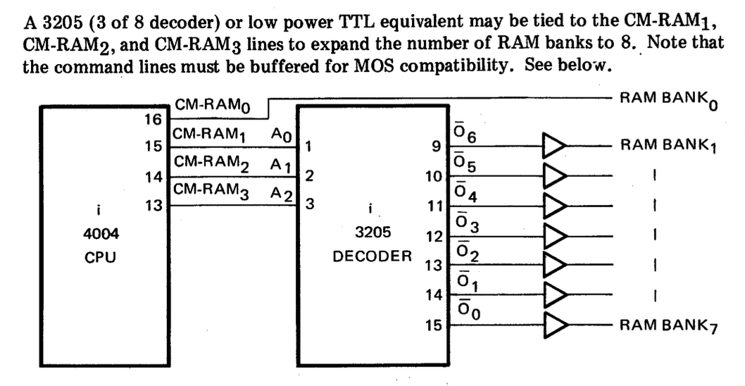
It is also interesting that the 4004 has no addressing modes, not even the concept of that exists. Its support for memory is rather rudimentary, in fact. It is also rather unlike what modern chips do, so I'll explain it. First of all, there can be up to 8 banks of RAM. Up to 4 banks can be supported without any external decode circuitry, and up to 8 can be supported with an external 3-to-8 decoder. How can this be? The 4004 has 4 CM-RAM outputs, which are basically RAM bank selects. If banks 0..3 are selected, only the respective CM-RAM line will be active during the proper time. If banks 4..7 are selected, a combination of CM-RAM pins is activated, but no combination includes CM-RAM0. Thus 7 combinations are possible, but of them one is all zeroes (unused), and three are a single active line (already accounted for above), thus there are four more combinations possible here, and they are used to encode banks 4..7. In reality, one could expand this infinitely, simply by using a few external latches and some OR gates to only pass the select signal to some chips but not others. I am not aware of any design that did this, but I verified that this works as you'd expect. The 4004 only has one CM-ROM (ROM select signal), and thus can only natively address just 4096 bytes of ROM. Here, too, with minimal external circuitry one could expand this to more.
4001 and 4308
Intel intended the 4001 to be the ROM for the 4004. It is a mask ROM that holds 256 bytes of data and contains a 4-bit I/O port. Each 4001, internally, knows its own "ROM number". What is that? Well, the 4004 can address 4096 bytes of ROM and the 4001 only holds 256. Logically one would need 16 4001s to fill the address space, but since there are not 16 chip selects coming out of the 4004, how would each ROM know when it is addressed? The last nibble transferred from the CPU on the bus during the A3 phase is compared by each 4001 to its internal "ROM number". If it is not a match, the 4001 will do nothing more till the next instruction cycle. If it is a match, it will consider itself active and provide data the 4004 requested, from the address it got during the A1 and A2 bus phases.
The 4001 is not programmable, it was meant to be custom-made for a customer. One would ship to intel the bytes one wanted in the ROM and intel would manufacture the 4001 containing those bytes - they are physically wired into the chip via its metal mask. The same applies to the I/O port on the 4001. It is a 4-bit wide port, and each pin could be an input or an output; have a pull-up, pull-down, or neither; could be inverting or not. The diagram shown here shows all the options. Each depicted switch could be closed or open. Some combinations, of course, make no sense, and intel warns so in their datasheet.
If you happen to buy a 4001 on eBay, you have no idea what its port config and "ROM number" is. You just have to test. Most ROMs out there are "ROM number" 0, which makes them especially useless for a home project. If they respond to address 0, then your code (presumably elsewhere in the address space) will never get to run. So why would you even buy a 4001 if it permanently contains code you cannot modify? Well, for the chance that it has an input port, since the 4002 does not, for some reason.
As I had mentioned above, the 4004 does not perform any memory operations - the other chips on the bus are expected to decode them and perform them if they are selected. The "selection" is made of a few parts. First is the CM-ROM line needs to indicate that this ROM bank is active during bus phase A3 (for code read) or X2 (for I/O ops). In the 4004, there is only one ROM bank, so this is always the case. The 4040 has two CM-ROM lines and thus one bank may be not selected. The second part of "selection" is whether the current chip in the bank is selected. This is determined from the last SRC instruction performed while this bank was selected. The chip thus addressed remembers this until another SRC instruction is observed while this bank is selected.
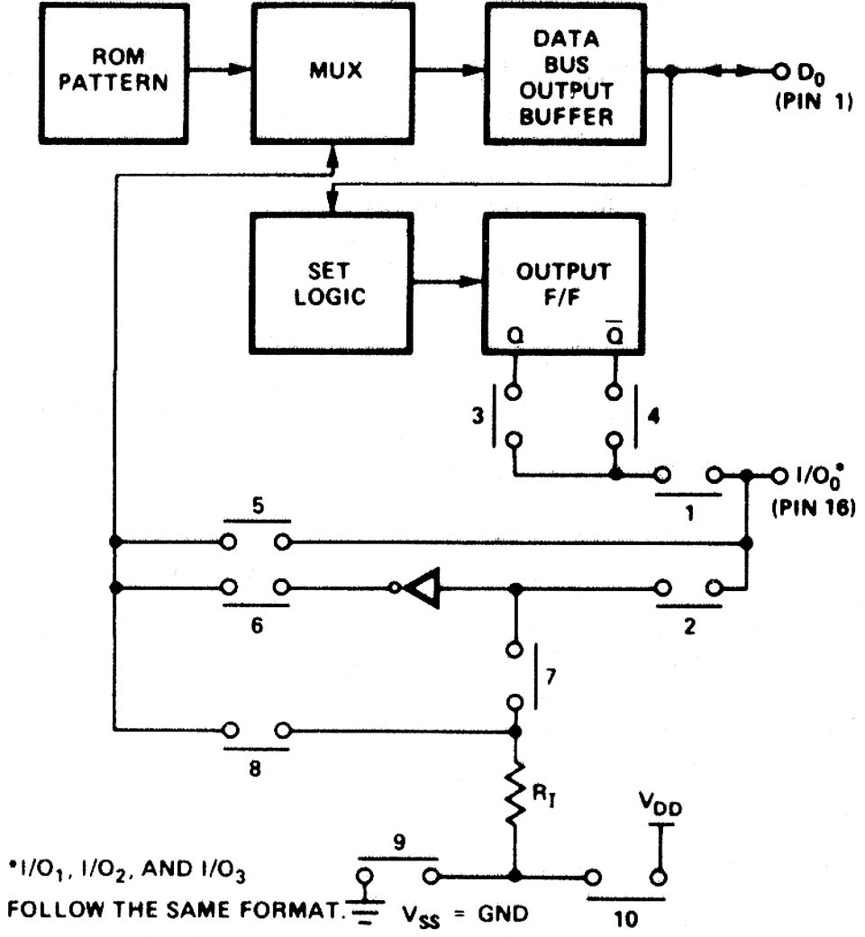
So, which instructions does the 4001 decode and execute? SRC is used to select which 4001 (of the 16 that make up a bank) is selected for I/O. The top nibble of the provided address (sent during X2 bus phase) determines which chip considers itself selected for I/O. Besides that, the 4001 only handles WRR (write ROM port) and RDR (read ROM port) instructions, and they do precisely what you'd expect from the names. As the I/O pins are not configurable and direction is locked at manufacturing time, there is no further config to perform. One curious thing is that when performing a read of the port, the I/O lines configured as outputs do not return the data they are outputting, instead they return a hardcoded value, that may be configured at manufacturing time to be either high or low.
The 4308 is basically the same as four 4001s in one package. It contains 1024 bytes of ROM and 4 I/O ports. It responds to four consecutive "ROM numbers". It is just a board-space optimization with nothing else interesting about it.
4002
The 4002 is the special memory for the MCS-04 system. It contains 320 bits of DRAM, refresh circuitry, and a 4-bit output-only port. I am not sure why intel made this decision, but this is so. Unlike the 4001, there is no mask ROM in here, so there would be no way to assign a "RAM number" to a chip. A different system is used. Each bank of RAM may have 4 4002s in it. So, logically, to determine a chip's index in a bank, we need two bits of information. One bit (the lower one) comes from the P0 input pin on each 4002 itself. The second bit is special per chip model. There are two: the 4002-1 and 4002-2. Thus a complete RAM bank, in order, will be made of: a 4002-1 with P0 = Vss, a 4002-1 with P0 = Vdd, a 4002-2 with P0 = Vss, and a 4002-2 with P0 = Vdd.
While the 4004 only has one CM-ROM output, it has 4 CM-RAM outputs, and as I mentioned above, this allows up to 4 banks of RAM without external circuitry and up to 8 with a single extra chip. So, a top-spec 4004 system without an extra decoder chip can have 16 4002s attached to it, for a total RAM capacity of 5120 bits (640 bytes). With a 3-to-8 decoder, the numbers double. In reality, memory addressing is not quite simple in 4004. So, if you were to only consider RAM you could address as a linear block that you could iterate over using a pointer, it is important to remember that each 4002 only has 256 bits of that. So a top-spec system would have 4096 bits (512 bytes) of that kind of directly-addressable RAM, assuming full 4 banks. I'll talk more about RAM addressing in the 4004 later. For now: each RAM bank is made of 256 nibbles addressable directly and 64 more, addressable weirdly.
So, what instructions does the 4002 handle? SRC, again, is used to select the chip in the current bank, both for I/O as well as for memory access. The top 2 bits of the 8-bit address sent select one of chips in the RAM bank. RDR, ADM, and SBM all read the nibble addressed by the last address sent via the SRC instruction. RD0, RD1, RD2, and RD3 read the status nibbles (more on them later). WR0, WR1, WR2, and WR3 write the status nibbles. WRM writes the SRC-addressed nibble - it is the opposite of RDM. The only other instruction the 4002 executes is WMP (write memory port), which sets the output value to be presented on the 4-bit output port of the currently-selected chip. The value will keep being outputted till another is written.
Sadly, there is no 4308 equivalent for RAM - there is no chip that would act like a full bank of RAM for the 4004. The 4265 can sort-of come close, but not in a fully compatible way.
4265
The 4265 is a general-purpose I/O device designed for the MCS-04 system. It has 4 ports of 4 I/O pins each and supports a number of modes of operation. You can peruse the intel docs on it at your own leisure to read about all the modes. I will only tell you about mode 12, as it relates to using the 4265 for RAM. In mode 12, the 4265 takes up an entire CM-RAM bank and responds to all 256 addresses that a SRC instruction might send. It can be interfaced to a 256x4 SRAM and it will read and write precisely like 4 4002s would. But wait, there is more, since 4265 in this mode also has 2 chip select pins that can be set to arbitrary values. If one were to use them as address lines too, one can interface a 1024x4 SRAM, which is a lot more RAM than a single RAM bank of 4002s could ever hold. Indeed, one would need to switch pages in this bank, as only one 256-nibble view is available at a time, but this is still pretty cool. The reason as to why this is not fully 4002-compatible is that there are no "status nibbles" here, so a 4265 + 256x4 SRAM is not a full replacement for a bank of 4002s if the code at all uses "status nibbles". When I talk about how they work and the advantages of using them, you'll see why this matters. Additionally, while the 4265 indeed has as many potentially-output port pins as 4 4002s would have, the way to control them is also not compatible (and, in fact, if you use 4265 for RAM access, you end up with no general-purpose output pins at all).
So, which instructions can the 4265 execute? SRC is decoded, as always, to handle inputting an address, of course. WMP (write memory port) is used to select the 4265 mode. In mode 12, RDM, ADM, and SBM will read the addressed nibble in the addressed page of memory. RD0, RD1, RD2, and RD3 select the given page, and then do a read. WR0, WR1, WR2, and WR3 select the given page and then do a write. WRM writes a nibble at the current address in the current page.
4008, 4009, and 4289
Given that intel will no longer manufacture you a 4001 with your custom contents (I called and asked), and the fact that the MCS-04 bus is rather strange and no other memory chip supports it, one might expect that one will need to do some perverted things to run code on a 4004 today. Of course, a simple FPGA, or even a modern microcontroller with a lot of level shifters could manage to pretend to be a 4001, but this is considered cheating in my book. Luckily, there is another way. There are two, even! Intel created a two-chip solution for a 4004 system to interface to normal garden-variety [[E]EP]ROMs: the 4008 and 4009. The 4008 handles the addressing part - it understands the MCS-04 bus protocol enough to tease out a 12-bit address that the CPU wants to read and can output that on 12 pins. Fancy that! The 4009 also understands the MCS-04 bus protocol, and it decodes memory instructions and generates control signals to handle I/O, ROM reading, and, optionally, writing in some weird ways that I prefer not to think about. It will also latch the 8 bits of data that represent an instruction and dish it out to the 4004 four at a time, as needed. The 4009 understands the same instructions as the 4001 does, except that instead of the I/O port being hardcoded at the intel factory, each write and read is output 4-wide to the outside world, to be dealt with as desired. This allows for a lot more flexibility. There is one more instruction that the 4009 understands that the 4001 does not: WPM (write program memory). This was meant for situations where the backing store was not [[E]EP]ROM but SRAM (eg for development). It works in weird ways that are beyond the scope of my lecture.
The 4008 and 4009 still need level shifters to connect to normal memories, since they were designed for the 15V EPROMS intel made, like the C1702A. The 4008 and 4009 are also rather hard to obtain nowadays. Luckily, intel also produced a combined chip - the 4289. It is basically a 4008 and a 4009 in one package, with level shifters built in. It can communicate with memories at 5V signal levels! This makes using a 4004 today pretty easy - a 4289 and a 5V 4096x8 [[E]EP]ROM is all it takes, really. The I/O story on the 4289 is also pretty simple and 5V-compatible. There is a pin that goes high when the CPU does an I/O read, and the 4-bit "I/O port" selection is available on 4 pins. Another pin goes high when the CPU does an I/O write, and the data appears on the I/O pins. In theory, this allows connecting up to 16 4-bit input ports and 16 4-bit output ports to the 4004, using simple buffers and decoders.
Using memory, and those "status nibbles"
The 4004 has no concept of addressing modes or even pointers, as I said. The way it addresses and uses memory is rather ... strange. Before you address memory, you need to select a memory bank. To select a RAM bank, one puts the bank number (0..7) into the accumulator and then executes a DCL (designate command line) instruction. This determines which CM-RAM line(s) go active during memory ops, and this selection remains active until another DCL instruction is executed. If no DCL is ever executed, bank 0 is used. There is no way to read back the current bank.
Each RAM bank (if fully populated), is made of 4 4002s. Each 4002 is made of 4 "registers". Each "register" is made of 16 addressable nibbles and 4 status nibbles. What do I mean by that? Well, if you were to read (using, say, the RDM instruction) memory in a bank from address 0x00 to address 0xFF, you'd first read nibbles 0 through 15 of "register" 0 in the 0th 4002, then the 1st "register" in it, then the 2nd, and then the 3rd. You'd then read the 0th "register" in the 1st 4002, and so on. Thus you'll have accessed every addressable nibble. Note that you did not access any of the "status nibbles" thusly. Those are accessed differently. With any address in a "register" selected, RD0 will read that 0th status nibble attached to this register, WR0 will write it. RD1, RD2, RD3, WR1, WR2, and WR3 work similarly, as you'd imagine. Note that the status nibbles are thus not pointer addressable in the normal sense. They are also not accessible to ADM and SBM instructions, and thus to do any math on their contents you must first directly load them into the accumulator.
As I explained, accessing memory is a multi-step process. As the 4004 has no concept of memory addressing, that is left to whatever memory device is attached to the bus. All memory devices watch the bus to see if their CM-RAM (or CM-ROM) line is active during the X2 bus phase. If so, that means a SRC instruction is executing. All selected memory devices will receive 4 bits (high nibble of address), and then on the next bus phase (X3) they will receive the next 4 bits (low nibble of address). They will store this internally, and use this address for all future I/O instructions, until another address is sent using SRC. A curious little quirk of this is that every memory bank has its own "current" address, since only the selected bank will interpret a SRC instruction seen on the bus.
So by now it should be clear that to read a nibble at address 0xAB in bank 3, one might have to do something like what you see here on the right. Best case is just one instruction. This only happens if you already had the bank and the address selected. This is unlikely. Second-best case is 2 instructions. This only happens if you happened to have the address already in a register pair, so you only need to execute a SRC before your RDM. If you did not, you'll need to use a FIM and clobber a register pair to get the address into it before using SRC. And if you also are not sure you have the desired memory bank selected, you might also need to load the proper bank number into the accumulator and execute a DCL. Realistically, you'll often end up with the case of FIM + SRC + LDM, which takes up 4 bytes of code and 4 instruction times. Yes...slow
Now let's imagine doing some math (say an addition) on larger (say 32 bit) values. Obviously, we'll store them little-endian. This'll help us since math happens from LSB to MSB, and thus we'll want to increment the pointer. This is much easier than decrementing it, since INC instruction exists, but DEC does not. We'll also assume our value does not cross a 16-nibble boundary, which makes our address incrementation much simpler. You see that code here on the right. Quite verbose. The total useful work here is 1 carry clearing, 8 loads, 8 load-adds, and 8 stores - a total of 25 useful instruction cycles. This code will, in actuality take 91 instruction cycles. The main culprit, as is clear, is the need to constantly increment pointers and manually send them onto the bus. This situation gets a LOT worse if you are not able to guarantee that the values do not cross a 16-nibble boundary. In that case a simple INC will not do, and a more complex construction will be necessary.
The issue is not limited to math. A simple implementation of memory copying looks similar and wastes similar amounts of time selecting memory addresses and incrementing registers. As you can imagine, this gets slow very quickly. If you keep some global state in some variables, to access each you need to first waste 2 instruction cycles to load its address into a register pair using FIM, then use one more to send it onto the bus using SRC, and finally you may read it using RDM or write it using WRM. If you have a few global variables that are often used together and in a particular order, you could order them in memory such that accessing the second one does not require using 2 instruction cycles on a FIM, instead using a single INC on the lower nibble of the address you had already loaded. One instruction cycle saved, but you still do need a new SRC. Basically almost every memory access is a 2-instructions-minimum affair, due to the requirement of a SRC. For the nitpicky of you, yes, indeed, a read-modify-write of a nibble need not employ a second SRC, but this is rare.
This is where those status nibbles come in handy. Instead of storing your globals in normal memory, you can stash them in status nibbles. Then, a single SRC, targeting any of the 16 nibbles of the "register" they belong to enables them to be accessed directly using a single one-instruction-cycle instruction (RD0, RD1, RD2, RD3, WR0, WR1, WR2, or WR3). This is wonderful for data that is often accessed, and once you realize the speed advantages of these "status nibbles" you'll want to use them everywhere! This realization allowed me to speed up the 4004 MIPS emulator by a factor of 30%!
Performance and clocking

All 2-byte 4004 instructions execute in 2 instruction cycles. All but one 1-byte instructions execute in 1 instruction cycle. The exception is FIN which is a one-byte instruction but it takes two instruction cycles. What is an instruction cycle? It is composed of 8 clock cycles, each representing a bus phase. A1, A2, A3 are the first three, and they send the desired ROM address to the ROM, LSB first. Next are M1 and M2 where the ROM outputs the instruction to the CPU (and any memory devices which need to decode it), MSB first. Then come X1, X2, and X3. X1 is when the CPU does some of the work on the instruction. X2 if when I/O is done between the CPU and any memory/I/O devices, the top nibble of SRC's address is also sent during this phase. During X3 the CPU does more of the work for the instruction, and also, if it is a SRC, the low nibble of the address is put on the bus. During X3 the SYNC signal is active, allowing all devices on the bus to [re]sync and prepare for phase A1 of the next instruction cycle. The 4004 needs a two-phase non-overlapping clock at a speed of 740KHz. Intel 4004 manual states that 500KHz is the minimum acceptable clock speed, and I can confirm that 10KHz does not work.
How does one even generate a "2-phase nonoverlapping clock"? Intel documents a method using some 9602 one-shots and some transistors to generate the proper clock signals. For the reset signal generator they recommend a 7400 and a transistor and a lot of passives. You can see the schematic here. This is no fun for anyone. Luckily intel also made a chip that does this all for you - the 4201. It can connect directly to a crystal and will divide it down by 7 or by 8, producing a proper 2-phase nonoverlapping clock signals at proper 4004 voltage levels. This chip will also generate a good reset signal for all MCS-04 components and (if using a 4040) help implement single-stepping. This one-chip solution is much nicer than the original one intel recommended, if you can get your hands on a 4201.
Some more annoying weirdness
All MCS-04 components operate at a very strange voltage level: their supply voltage is minus 15 volts. Yes. They also use inverted logic on all pins. To indicate a zero, a pin will be grounded, to indicate a one, a pin will output negative 15V. So to any other chip, even with level shifting, the signals will all appear inverted. Chips do not really care what you call "ground", so instead of thinking that MCS-04 chips need "-15V", it is simpler to think of them needing "-10V" and "+5V" supplies, and they are just missing ground pins. This helps in systems that also contain the 4289, since with this exact setup it can interface to normal 5V [[E]EP]ROMs. This just leaves you with the somewhat-annoying problem of generating a few watts of -10V...
Initial planning
Let's make a dev board
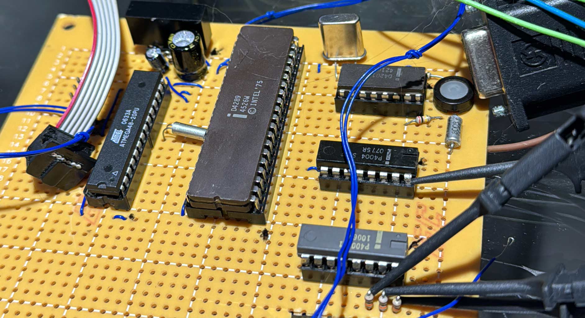
To make sure that I could even make a 4004 work correctly, I decided to build a simple dev board on a protoboard. It contained almost the simplest possible 4004 system: a 4201 clock generator with a reset button near it, a 4004 CPU, a single 4002-1 RAM, a 4289 ROM controller, and an ATMEGA48 to act as my ROM. The AVR is fast enough to pretend to be a ROM and easy enough to reprogram in-circuit using AVR ICSP. The board was powered by 5V, and I used an isolated 5V to 10V boost converter module to produce 10V. Its positive output was grounded, giving me a -10V supply to feed to the chips in addition to the +5V I already had.
My first attempt to turn the board on did not succeed. I set a conservative 100mA limit on my power supply, and the board was clearly trying to draw more. After verifying that, as far as I could tell, I did not mess anything up, I raised the current limit to 500mA and tried again. It worked. My simple program that blinked a LED connected to the output pin 0 of the 4002 via a 2K resistor worked and the LED blinked. Glorious! My first 4004 program worked from my first try!
Output is pretty easy - the 4002 has output pins. Input is a bit harder. The 4289 does support input, but it needs a tristate buffer since its pins are only inputs when the CPU executes an RDR instruction. It also needs a decoder to properly decide which of the 16 4-bit input ports it is reading. I was determined to avoid both of these things. After some math, I decided that I can make do with 4 input pins total. This means that I do not need any decoders. I also decided that if I put a 1K resistor between my data sources and the 4289, that even if they try to fight, their abilities to hurt each other will be limited by the resistor. This should allow me to avoid needing a tristate buffer. This all turned out to work fine. For my proto board I used a single FET with a resistor as my level shifter. On the final board I used a CD40109B.
Emulating my 4004 system

I had many doubts that I could fit an entire DECstation2100 emulator into 4KB of 4004 machine code. 4004 is very verbose, and operating on nibbles means that basically any operation ends up needing a loop. I was, however, very determined. To save myself the disappointment of developing hardware only to find that the software is impossible, I decided to start with the software. First, I needed an assembler. I was about halfway through writing my own when I stumbled onto A04. It had a number of annoying bugs (eg: it errors out when a JCN or an ISZ is on the last bytes of a ROM page, even if their targets are indeed reachable as they are on the next page). A04 had one major benefit - it existed, saving me the trouble of writing my own.
My next step was writing a 4004 emulator ("u4004"). This involved some experimentation with the hardware to clarify a few things that had not been clear in the datasheet, for example: how carry flag works in subtraction. Initially the emulator only emulated the 4004 and normal memory, but over time, it grew to properly emulate the complete system I intended to build - a virtual SD card, a virtual SPI UART chip, a virtual VFD, and the same layout of 4002s as I planned to have. This did not take a lot of time, since the 4004 is laughably simple. I do not think it even took a week to write and debug the core of the emulator. Emulating the peripherals took longer, as did writing the code that would parse SPI out of I/O pin states and flag any errors. I REALLY did not want to debug this on real hardware. The closer I could come to it in emulation, the better! Here you can see a screenshot of u4004. It shows the serial console output, the VFD display, and the PC LEDs (more on all this later). It also shows how much real time would pass on a real 740KHz 4004 system to get to the current state.
The MIPS emulator
Why MIPS
Of course, Linux cannot and will not boot on a 4004 directly. There is no C compiler targeting the 4004, nor could one be created due to the limitations of the architecture (go try to fit all of the Linux kernel into a call stack of no more than 3 levels deep). The amount of ROM and RAM that is addressable is also simply too low. So, same as before, I would have to resort to emulation. My initial goal was to fit into 4KB of code, as that is what an unmodified unassisted 4004 can address. 4KB of code is not much at all to emulate a complete system. After studying the options, it became clear that MIPS R3000 would be the winner here. Every other architecture I considered would be harder to emulate in some way. Some architectures had arbitrarily-shifted operands all the time (ARM), some have shitty addressing modes necessitating that they would be slow (RISCV), some would need more than 4KB to even decode instructions (x86), and some were just too complex to emulate in so little space (PPC). ... so ... MIPS again... OK!
A start
I started with emulating just the CPU, to evaluate how much space that would take and help me estimate the feasibility of the project in general. As this was my first time programming in 4004 assembly, I had no feel for how dense the code would be. Initially, I skipped dealing with RAM and just assumed that the "current" MIPS instruction will be in r8:r9:r10:r11:r12:r13:r14:r15 registers, MSB-to-LSB. Yup...half of the registers are used just to hold the instruction. I considered using memory for this, but the values would need to be used in many ways in many many places during decode, so that would turn out to be messier. Plus, I still had 8 registers left, that is two more than x86 ever had! Of course, "assume the instruction ends up in registers" is not testable, but that was not yet the goal. Initial dispatch (based on the top 6 bits of instruction) to a 64-entry (128-byte) table of unconditional jumps took 13 instructions, including the JIN that it ends with. So 128 + 13 bytes just for that. That is already 3.4% of the entire code space I had. Not a great start. Top level opcodes 0 and 1 each need another sub-table to decode. One table will have 32 entries and the other will have 64. They will need 12 and 14 instructions respectively to calculate the jump target. Thus once we've more or less handled the majority of the decode, we've used 128 + 128 + 64 + 13 + 12 + 14 = 359 bytes of code space. That is over 1/12 of the entire code space, and we have not yet even executed anything. Yeah... It was, of course, approximately at this point that I realized that this project will be harder than I had anticipated. But, no surrender!
MIPS has 32 user-visible registers, of which the first is the zero register, writes to which are ignored. 32x 32-bit registers is 1024 bits of register state. This is 256 nibbles, which, in 4004-land, is one full RAM bank. So there we have it: bank 0 will have MIPS register state. MIPS has a delay slot, so in addition to PC we also need to store NEXT_PC so that we can properly handle branches and the delay slots behind them. As PC is not part of the general 32-register bank, these two account for 16 more nibbles of memory (in bank 1). For memory translation, MIPS has a TLB (read more about that here), where each entry is 8 bytes long and there are 64 entries. This would take up 4 complete memory banks. And to access an SD card we'll need at least a sector-sized buffer (512 bytes), which is also 4 memory banks in 4004 land. So we need at least 10 memory banks‽‽‽ No go! Beyond 4 banks, the 4004 needs extra chips; beyond 8 banks we'd be cheating. There must be another way! I decided to punt this problem to later as well.
As I continued writing the emulator, the code memory was filling up fast. Most things took a lot of operations, requiring a lot of loops. Some things were very hard due to the way 4004 works and its lack of status flags. Detecting signed overflow was particularly hard. And, of course, 32x32->64 multiply was a huge pain. The signed variant was even harder. I was very glad when it was over, at least I was until I had to implement division. In some cases, signed 32-bit division can take up to 80,000 instruction cycles thanks to needing to operate on only a nibble at a time and ISA design of the 4004. That is almost a second of realtime to perform a division. Realizing this gave me an idea to show PC in LEDs, which I will get back to later.
Logical ops
I have never before seen a CPU that lacked ability to do basic logical operations, until I saw the 4004 manual. The 4004 lacks ability to do any of them. There is no logical AND, no logical OR, and no XOR. Intel, helpfully, gives sample code in their 4004 programming manual to implement those logical ops on nibbles, but I was able to produce more compact and faster routines. Nonetheless, it takes dozens of cycles PER NIBBLE to do this! How does one even do this? Observe that if we were to isolate a bit from each operand into a register's lower bit (the higher ones being zero), and then add those registers while input carry flag is zero, the result's bit 1 would only be high is the input's two bits were both ones (AND). The result's bit 0 would only be high if the input's bits differed (XOR). If we did the addition with input carry being one, the result's bit 1 would be high if either of the inputs was a one (OR). This is the basic building block of implementing logical ops in the 4004. The rest is looping and shifting! And then, you remember that each MIPS register is 32 bits long, and a whole lot of cycles are going to go into doing all of this per-bit!
In addition to the usual suspects of AND, OR, and XOR, MIPS also has NOR. Luckily it is easy to compute in a similar way. One might ask if there is a way to speed this up using some sort of a lookup table? Yes, but a table with 256 entries is 1/16 of the available code space. Three such tables would take up 3/16 of the available code space. That is a lot of code space to give away in a project where I was not sure I could even make the code fit in as is. So this idea was shelved.
Shifts
MIPS has the usual complement of shifts: left, arithmetic right, and logical right. They can be by a fixed amount (encoded in instruction) or a variable amount (taken from a register). The second part of that is trivial, we can find the right register and read its value. To the emulator, all shifts are by a variable amount between 0 and 31. Again, the 4004 makes this rather hard. The only shifts it has are shifts by one through the carry flag. So to shift a 32 bit value by one bit, we need a loop with 8 iterations. Thus to shift by N bits, we'll need to run that loop N times. This is getting pretty slow, eh? But wait, there is more. Arithmetic shift right requires the new MSB be the same as the last MSB. The 4004 lacks a way to do this easily, so it takes a few extra instructions to set this up every iteration. Thus, shifts are slow, and they get slower as you need to shift by more bits. One could come up with many clever ways to optimize this, but I was optimizing for code size above all else!
Space optimization and 4004-specifics
As you may recall, I mentioned that the 4004 has 4 levels of stack, and that one of them is always used as the current PC. This means that if you call into 4 levels of subroutines, you'll not be able to return all the way out to the last. This is annoying, but palatable. However, this also has another fun consequence. Because the 4004 treats the stack as a 4-entry circular buffer, you CAN have an unbalanced number of calls and returns. I use this to save some space in my code. When a MIPS instruction's destination register is $zero, the result is discarded. For speed and code size, I emulate an actual $zero register, and just ignore writes to it. This is faster and simpler than replacing all reads with zeroes as on MIPS more registers are read than written. Now, you might imagine having a isZeroReg() function, and after it, a conditional jump based on its output. If it says "yes", go handle next instruction; if "no", continue processing the current one. This would be suboptimal, since every callsite would need this conditional jump. My idea is better. My checkZeroReg() just goes to the handle_next_instr label if the destination register is $zero, and does not actually return at all. It only returns back to the caller if the destination register is not $zero. This means that every instruction targeting $zero pushes yet another value unto the 4004 stack that will never be popped. However, as long as you do not have too many returns, it is safe to have too many calls. This saves three bytes at every callsite, which there are close to a hundred of. Saves three cycles too! This was a big deal in my increasingly-cramped ROM.
There is curious little part about emulating MIPS: When, exactly, can you stop working on an instruction that targets the $zero register? For instructions with no side-effects, you can skip doing any work at all. So for example an ADDIU or an SLL can be skipped entirely. This is not true for instruction that might trap, like ADDU. Here, some work is needed up front - to check if the instruction might overflow and thus need to cause an exception. In my emulator I do this check, and then skip the actual addition if the target is $zero. Why someone might have such an instruction in their binary is another question, but as an emulator writer, correctness is important. Memory load instructions are similar. They might cause an exception, so even if they target $zero, the memory translation and access need to be executed to make sure they succeed (or to cause them to fail as they should). The only part that can be skipped is the final copying of the loaded value to the destination register, and the potential sign-extension.
Hypercalls
To connect the MIPS emulator to the outside world, hypercalls are used. This allows me to not have to emulate SCSI disks, for example. The hypercalls are actually the same as in the LinuxCard project. They mainly concern accessing storage using the PVD Linux kernel driver and outputting characters for early boot logging. So far, this is sane...
Second-order hypercalls
But, as I had mentioned, I developed much of this code not on real hardware but on an 4004 emulator I wrote (u4004). This made development easier, since I had not yet even built a board with a real 4004 yet. Indeed it is emulators inside emulators. It is emulators all the way down, in fact. In any case, the 4004 emulator also had hypercalls. Initially, before I properly emulated the SPI-attached SD card, UART chip, PSRAM, and VFD, they literally accessed the host file that pretended to be the SD card and printed to console to display text via hypercalls. This allowed me to focus on the actual emulation bits without worrying about the accessing the real world.
It is tight
By the time the CPU emulation was complete, there was only about 400 bytes of free space left in my code space allowance of 4096 bytes. And there was much left to do. Since I planned to use a paravirtualized disk driver for Linux, the only peripherals I would really need to emulate would be: the DEC bus fault reporter (reports bus fault address), DZ11 (serial port), and DS1287 (real time clock and timer). The first one is simply a register that can be read. Easy enough. The next two were harder. Luckily, I had a normal MIPS emulator that could boot Linux from the LinuxCard project. I started chopping it up to minimize how much emulation is done of each of the peripherals, until I had them both minimized down to almost nothing. For DS1278, Linux was willing to live with it even if all registers read as zeroes, writes were ignored, an interrupt was periodically delivered, and it was deasserted upon reading of a status register. I decided to do just that - deliver an interrupt every 65,536 MIPS instructions to the emulated CPU. On the DZ11, there was a bit more work, but I was able to cut away all the channels except the zeroth, and to simplify much of the logic and remove all receive and transmit buffers. I also cut down the IRQ capabilities of the R3000 CPU. Only two IRQs are used in this system - RTC and UART. I removed the capability for all others to work at a great speed and code size gain.
With the peripherals successfully minimized, I went on to implement them in 4004 assembly. At this point in time, there was 200 bytes of ROM left, but Linux could boot entirely inside the emulator inside the other emulator! The main problem was that there was no code to actually talk to the real hardware I would have to use: SD card, PSRAM, VFD, UART chip. And 200 bytes is a bit tight for all of that. But, I was determined to try!
SD card driver and the last of the ROM space
So, I added a virtual SD card to u4004, connected to a virtual SPI bus, the three output pins being three pins on a virtual 4002, one input pin being the lowest input on a 4289. I then went on to write what I believe to be the world's smallest SD card driver in existence. It fit into 190 bytes and would successfully init a card, get its size, and allow sector read and write. I also tried this driver on my dev board from earlier, connected to a real SD card, and found that it worked! Woo hoo!
I had 10 bytes left in my ROM and a lot more code to write. I scrounged hard and made a little more space - 44 bytes of ROM were free. I then re-read all the docs and saw that on reset, every 4002 will zero its memory, so I did not need to spend code clearing memory on boot. This saved another 12 bytes. 56 bytes free! Still, this was clearly not enough for what I had left. Failure!
The emulator needs more ROM
How to make ROM banking work
Well, OK. I can have 8192 bytes of ROM, in two banks, flippable by a pin controlled by a 4002. Jumping between them would take a little work, but it could be done. And there would finally be more space! The way the bank switching would work is that after the bank output pin is written using WMP, the next instruction would be fetched from the other bank. This means that the call-gates had to be precisely positioned in both banks. Additionally, 4002 outputs reset to outputting 0, which in MCS-04 means the higher output voltage. Practically, this means that the board would boot from bank 1 and not bank 0. Oh well, that is solvable with a cross-bank jump. Calls between pages are also a bit complicated, since the return value is only valid in the page where it originated. So instead of a JMS to a function, now I'd JMS to a veneer that would switch banks, continue in the other bank, JUN to the function, it would JUN at the end to a return veneer, which would swap the banks back, and only then BBL to return. This mess was necessary to not burn one of only three call depth levels available in the 4004. Messy but it worked!
Now that I have space...
Suddenly I had mode space! So many possibilities opened up! So many pieces of code that had once been optimized for space could now be optimized for speed. There were limits, of course, since jumps between ROM banks were a pain, so only a few things initially got moved. The first were the logical operations. AND, OR, and XOR each got a full 256-entry lookup table in the second ROM bank. How does one implement a lookup table on the 4004? Since the result is a nibble, just a table of BBL instructions is good enough, at a 256-byte boundary. A jump into that ROM page at an index whose high nibble is one input nibble and low nibble is the other input nibble would jump to the BBL that would populate the accumulator with the result. However, if the entire ROM page is filled with BBL instructions, how does one jump to them? Recall that the computed jump instruction JIN had a curious footnote in the manual: if it is the very last instruction in a ROM page, the address that the jump is relative to is not the start of its page but of the next. The 4004 manual warns that this is hard to use and should be avoided! Well, I found it wonderfully easy to use and used it to great success. Then, the functions to AND, OR, or XOR full 32-bit values were simple to implement and ran much faster.
Multiplication was another case where a table could help, but this is slightly more complicated. A nibble times a nibble can produce up to a byte of result (0x0f x 0x0f = 0xe1). This means that the trick with a JIN at the end of a page followed by a page full of BBLs with correct value would not work. Well, there is also the FIN instruction which loads a whole byte from ROM into a register pair. In fact, it also has the same quirk with regards to the addressing, so that placing it at the end of a ROM page would indeed allow using the entire next ROM page as data. Wonderful! There is one problem: FIN is not a return statement, so after it performs the load, it will continue executing the next page's data as instructions. This is most unpleasant! There is no way around this in the general case, but I am not seeking to solve the general case. If we imagine a LUT for multiplication, the first 16 entries will be zeroes. So, if we can simply assume that our larger multiplication implementation does not call the LUT for zeroes, then we can simply FIN and then BBL safely. This is what I did, in fact. Multiplication got 8x faster compared to the one-bit-at-a-time implementation I had had before.
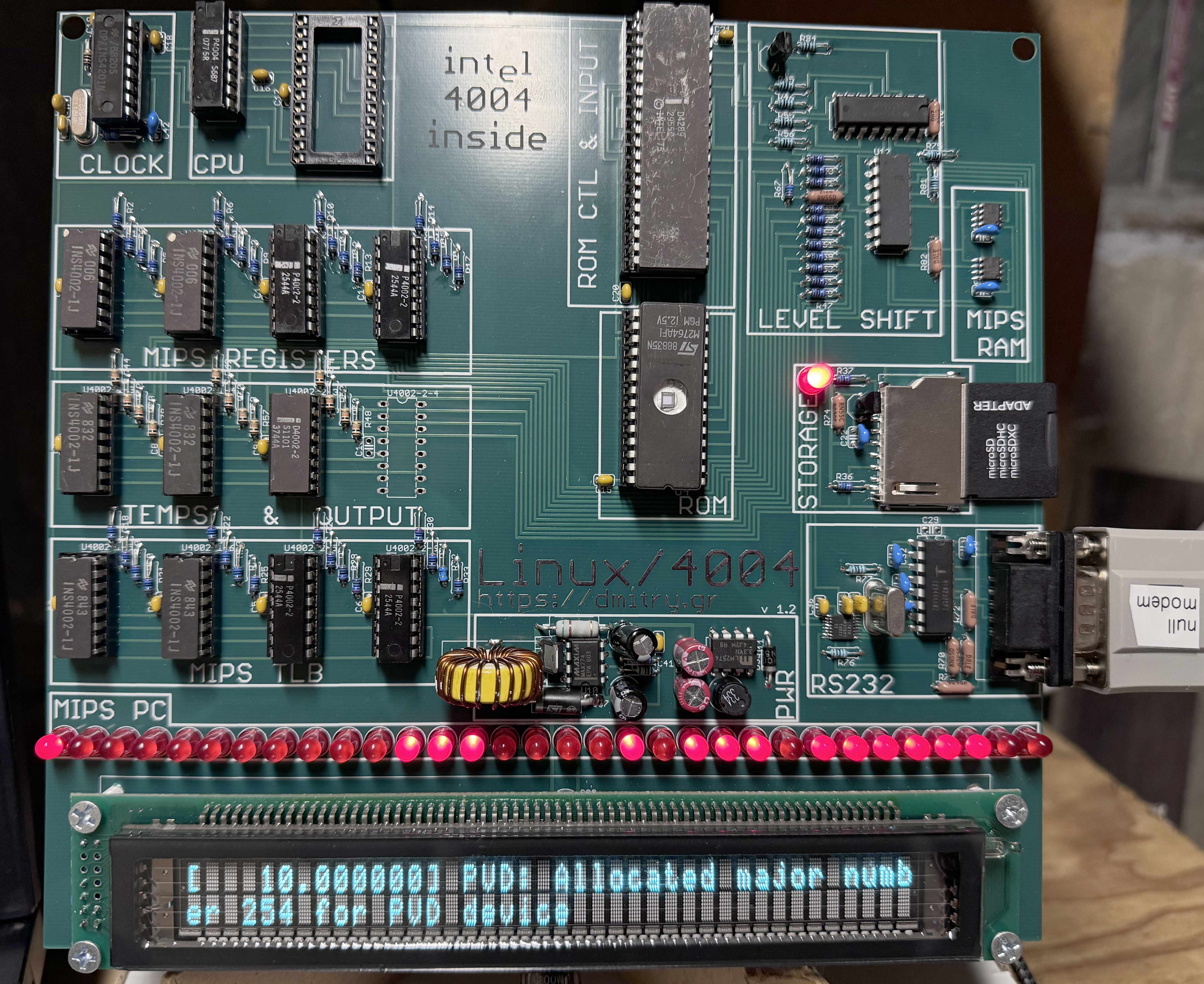
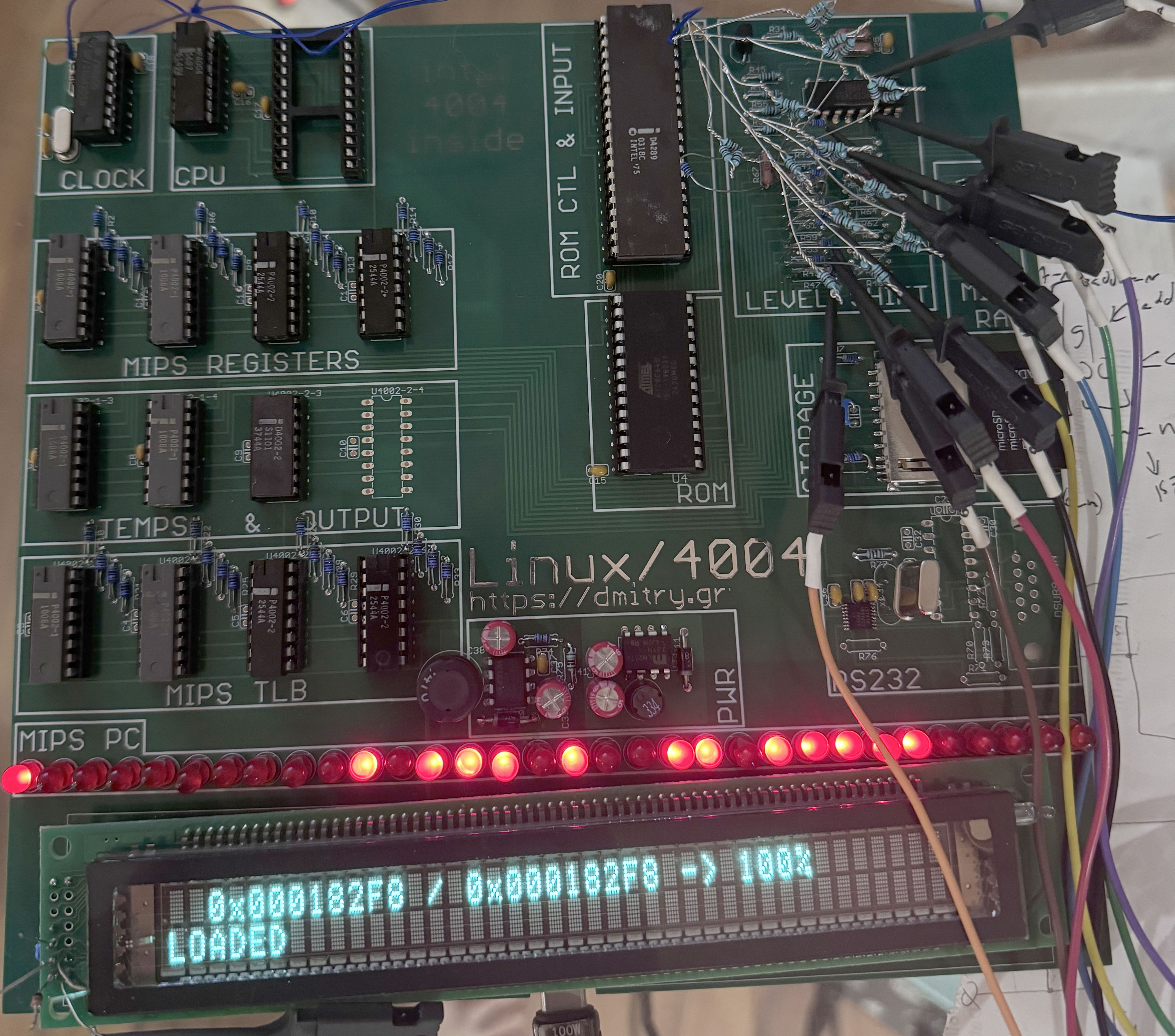
Hardware
At this point, it was becoming clear that the project was feasible, and so it was time to build some real hardware! I decided that the final result should be artistic, recall the 1970s, and be able to be hung on a wall and look pretty! The board would be composed of all through-hole components, thick right-angle-only traces and no vias anywhere for a classic look. Moving on to parts selection...
SPI PSRAM
Unlike the last time I did this, I had no desire to manually refresh DRAM. Since 2012, wonderful SPI PSRAM chips have appeared from AP MEMORY, ISSI and Vilsion Tech. They are easy to work with and require many fewer pins. I decided I'd use them. They are not through-hole, but they are small and I was willing to compromise. Plus, since I had already written code to do SPI on the 4004, I could reuse it. I wrote an emulator of SPI PSRAM and added it to u4004, so that I could then test my PSRAM driver. It all worked rather well, after I properly remembered that 4002's outputs are inverted. Sadly, emulating a real bit-banged SPI interface slowed the emulation by a factor of two, compared to a magic "fetch an instruction" hypercall I had had. Doing things more realistically is always slower. Fetching an instruction, on average, took longer than emulating it now. Sadly, such is life. I considered using full QSPI mode, but I'd need a lot more input pins than my plan called for. I could easily use a 4265 to do this, and speed gains would be nice, but I sought a project that could be reproduced by others. 4265s are rather hard to get, so I decided to do without it.
The SPI PSRAM needs time to refresh the internal DRAM, and because of this, there is a minimum time it needs to be left alone between instances of being selected. This would not be hard to meet with my emulator being so slow. It also has a maximum length of time it can be selected, so that it is not blocked from refresh for too long. This limit is 8 msec. I worked hard to meet this time by instrumenting u4004 to keep track of selection length. It is, of course, at this time that I rewrote all the SPI code many times over for speed. Now that I had space in ROM, I also inlined a few uses of it and unrolled some loops. The final clock speed I attained on my bit-banged SPI out a 4002 was about 7.4KHz. Not too fast. Luckily, as per u4004, my longest selection of RAM was 7.4 msec, so I was meeting the datasheet-imposed limit.
A later re-examination of the datasheet showed a slight issue with all of the above. The unit in the PSRAM datasheet was microseconds, not milliseconds. Oops! So, I was not meeting the timings, I was blowing them by a factor of nearly a thousand! Luckily, this seemed to be causing no issues at room temperature. After some thought, it makes sense. Since there is a lot of time between my accesses, the chip likely has time to do multiple full-array refreshes between each of my selections. I ran a number of tests on an RP2350-based board severely downclocked and found no issues, so I guess it works well enough!
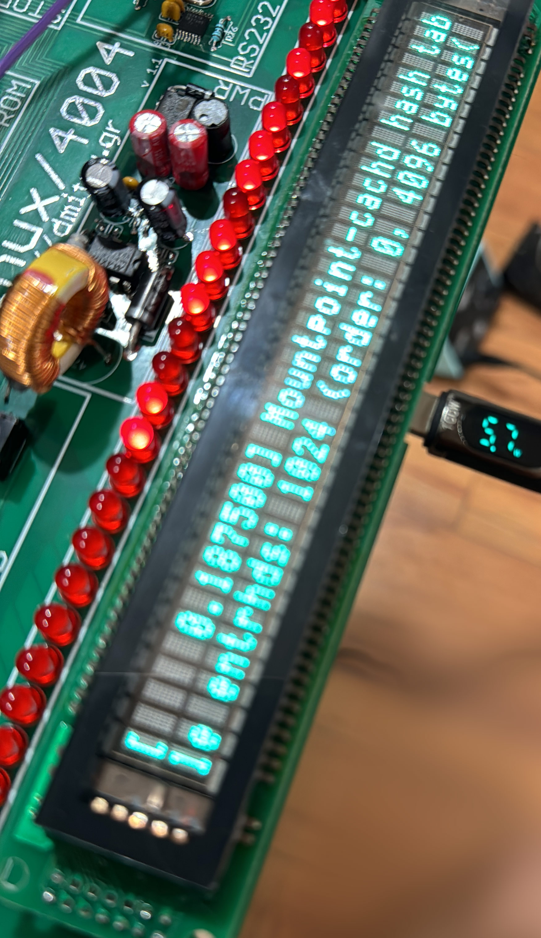
The VFD
I knew that I wanted the final hardware I build to be an art piece that I could hang on a wall, so merely having a serial port would not do. What could add more retro flair than a 40x2 VFD display? In my mind: nothing! I was able to locate a VFD display that could speak SPI and use a single 5V supply - a Futaba M402SD10FJ (I am told that Noritake CU40025-UW6J is compatible). After some experimentation, I found that it would also happily run on 3.3V! Even better! The protocol to talk to it was a bit strange, and not quite SPI. It used a single line for both input and output. This required some thinking, electrically, but at the end it was resolvable. Why would I need to read from a display? RAM savings. If I want to scroll the display, I need to copy the bottom line to the top line. There are two ways to do this. One is to buffer it and the other is to read it back. Buffering 40 characters requires spending a whole 4002 chip to do that - that feels like a waste when the display itself can support this functionality. At the end I was able to make it work and the display indeed displays the last two lines of output! It is glorious! One annoyance was that the VFD only operates in SPI mode 3, while all other devices I have use mode 0. Luckily, the assembly changes were minimal to support this, and u4004 was updated to support it too.
The UART
I was not going to implement a full keyboard out of buttons, though. I thought that this would be unsightly, plus I am lazy! I did, however, plan on having a real serial port on the board. There was one problem: despite much searching I found only one through-hole SPI UART chip (the MAX3100), and, sadly it had a fatal flaw. While it supported doing flow-control signaling, it lacked the ability to automatically signal the other side to stop talking when local buffer was full. Instead, its flow control outputs functioned like GPIOs that the host had to control. This was a nonstarter for me, since my host CPU was too slow to do this fast enough. After much soul-searching, I decided that the UART will be the third surface-mount component on this board. Given the option to use an SMT part, I decided on SC16IS741A. It has a large 64-byte buffer and can do flow control automatically, with threshold settings on when to signal stop and when to signal resume. Awesome! I do not use flow control on the TX side since my emulated MIPS CPU simply cannot produce data very fast.
I emulated the SC16IS741A in u4004 and verified that my code drove it correctly. I wanted to see both the VFD and the outputted serial data, so I wrote my first curses UI. It was amazingly easy and I am surprised that it took me this long to discover it!
The blinkenlights
Now that I had curses, I could add more things to u4004. As I have mentioned, the emulator was bound to be rather slow. So, why not, for extra retro flair, show the current PC using 32 LEDs? And if I were to do this, why not also emulate it so that I could verify correctness? I did! For speed, the emulator updates this only every 32 emulated MIPS instruction, which is plenty.
The easy level shifting
I planned to use the TEST pin on the 4004 to indicate that there was a character ready to receive from the UART chip. This would allow easily checking for it, using JCN T conditional jump. This level shift from 5V to 15V was done using a FET and a resistor - simple stuff.
To convert my various 3.3V signals to the 5V that the 4289 will accept as inputs, I used a CD40109B. It has a high input resistance and a low output resistance allowing me to play various tricks with resistors on the output and not worry about anything.
Actual RS232 serial port signaling requires some rather high voltages. There are standard chips for dealing with that, and I chose a cheap through-hole one: HIN232. It just needs a few capacitors to work. It converts two lines in each direction between high voltage inverted and low voltage non-inverted signaling. This allows for transmit, receive, and flow control in both directions to be level-shifted.
The hard level-shifting problem
All that was left was to convert the high-voltage outputs from the 4002s to my 3.3V domain. This turned out to be difficult. My first idea seemed simple but did not work. I reasoned as follows: the input is either -10V or +5V, the output should be either +0V or +3.3V. So if we create a resistor divider with ratio X and the other end of it is at voltage Y, what are the values or X and Y to accomplish the desired result? Two linear equations with two unknowns. Easy. The ratio needs to be around 1:5 and the other voltage needs to be around 2.8V. So, my plan was to use a pretty strong (few dozen ohms) resistor divider to create 2.8V out of my 5V supply, and then use a rather weak resistor divider (few dozen kiloohms) between each 4002 output pin and the 3.3V consumer of its output. This did not work.
I spent a lot of time wondering why. I recalled a very strange comment in the intel 4002 manual: "This port can be made low power TTL compatible by placing a 12K pull-down resistor to Vdd on each pin." This comment truly made no sense, since Vdd is at minus 10 volts and that is very much not TTL-compatible. I asked around, but found no satisfactory answer to this. When my voltage dividers did not work, I started wondering if what I had tried to do failed because of some mystery that that comment had been alluding to. I measured the raw outputs of the 4002s before my level shifting resistors and noted that while the high voltage output was indeed +5V, the low was not at -10V, instead hovering at -3V. This is rather odd, since there is no -3V supply anywhere in the system, and the only load on the pins was a 30kiloohm resistor. It was starting to look like the 4002 output pins simply could not sink any appreciable current. Maybe this is why intel suggested a pulldown? A better-informed look at the datasheet confirmed this. Intel specifies that the pins will sink 50 microamps only before they start being dragged up to Vss. At 3mA current sunk, they are only promising an output of Vss-4.85V, which is +0.15V - quite far from the -10V we expected! Suddenly it all makes sense. The pins can source plenty of current, and they will happily fight back against a 12K pulldown, but they suck at sinking current, and the pulldown would help them! It now all made sense! I guess "TTL compatible" was intel speak for "able to actually be connected to anything of consequence that is not a high-sensitivity oscilloscope". While I was sorting this all out with a healthy dose of guess-and-check, a lot of resistors sprouted over the board, as you can see in the image of the first-revision board there, in the state where it first fully worked!
Adding a pulldown, and then using a resistor divider from there ... to another resistor divider was starting to sound needlessly messy, and would likely not work. I came up with a new plan, which will duly horrify any EE. I would add the 10K pulldown, then, the output, via a 2.7K resistor would be used directly, clamped by two diodes, one to +3.3V and one to ground. For high-speed signals this would be problematic, but as MCS-04 chips are quite slow, it would be fine. I prototyped this and it worked well. To save space, I decided to use a TVS instead of 24 diodes. In any case, there was one small remaining problem: diodes have voltage drops, so clamping a signal to ground and +3.3V would in fact produce a signal that varies from -0.65V to +4.15V. Luckily this problem was easy to solve. A 3-resistor divider with low resistances was used to produce +0.65V and +2.65V to feed to the TVS low and high inputs. Did it work? Yes it did! Please take a moment to be truly horrified.
Power supplies
As can be seen, this board was going to have a lot of different voltage levels. I decided to provide power over USB-C edge connector, same as I did before. This takes care of +5V supply. I also needed -10V, and +3.3V. Limiting myself to only through-hole parts made things a bit complicated. Modern switch-mode controllers are very fancy and efficient, but they only come in surface-mount variants. I was stuck with very very old chips - the ones that were famous for being picky about layouts and would fail to work in fun ways if given an inductor or capacitors they did not like. It was a relief when my 3.3V step-down regulator based on LM2574 worked from the very beginning. The draw on it was a few hundred mA, split mainly between the VFD and the SD card. It caused no issues, which was nice.
My first revision board used a MAX764 as a inverted-step-up regulator. It worked fine for a little bit of early bring-up, but if I populated more than four RAM chips, the board would stop working. After scoping the regulator's output it became clear why - it was drooping from the requisite -10V to -7V. This would not do. After some investigation, it became clear that the MAX764 simply cannot supply all the current needed by this many MCS-04 chips.
The second revision board used a MAX774, which is basically the same chip as the MAX764, except that the main switch FET can be external, allowing for a beefier one. I also switched to a larger diode and a larger inductor. This worked - all the chips could be powered well. The inductor size is comical, and I asked some people who actually know this stuff why this is, since I've seen plenty of smaller modules that do the same thing I was trying to. The answer was basically that modern chips operate at much higher frequencies (in the MHz), allowing usage of smaller inductors. They are also usually designed by competent EEs, not by me. The MAX774 operates in the KHz frequencies, and thus needs much larger inductors. I was also told that my board layout could be improved, but there was not too much that could be done with through-hole parts and that I should just use a module or some modern regulators.
It also took some experimentation with inductors and capacitors to find ones that would produce low-enough output ripple while also not making audible noise. I am happy with the final result - it is silent, can supply over 700mA at -10V with under 200mV ripple.
How to debug the hardware
This is the 21st century!
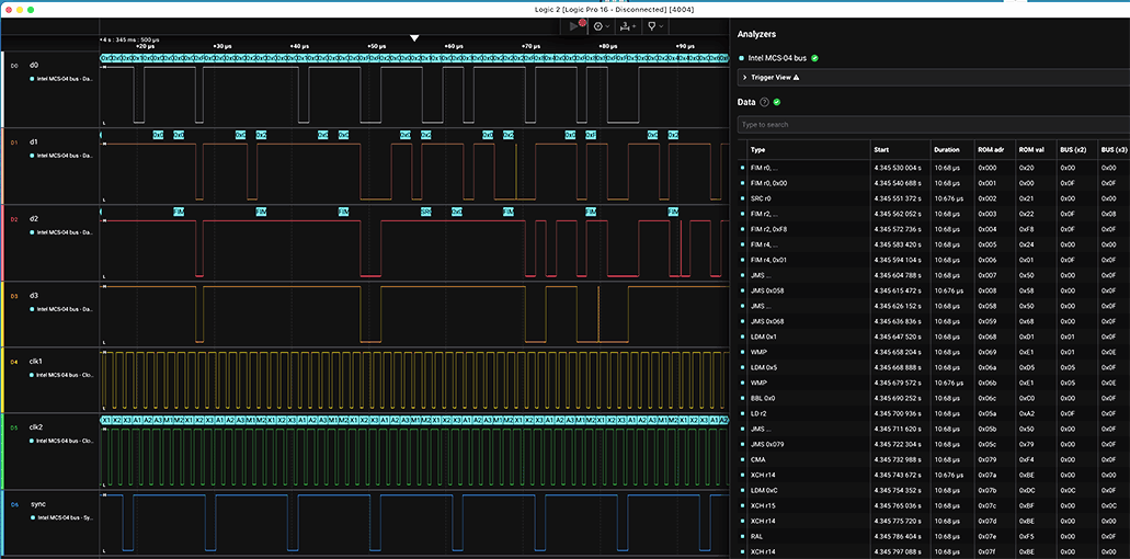
As you might imagine, the 4004 does not have any built-in debugging capabilities. Luckily, we do not live in the 1970s. You can go and grab yourself one of these bad boys and capture the entire MCS-04 bus for hours on end. Analyzing it might get a bit annoying, though. This is true especially if you are looking for a bug that happens a few million cycles in. It annoyed me enough that I wrote a decoder for the Saleae Logic Pro software that can decode the MCS-04 bus. It will show bus states, ROM addresses and values read from them, disassembly, and the value read from and written to RAM and I/O. It is part of the downloads at the bottom of the page here. Enjoy! EDIT: I contributed it to Saleae, and it is now part of the normal Saleae software, so no need to build it from my source anymore.
The garbled text mystery
Why did I need to debug the hardware? At some point in time I assembled a new revision 1.1 board. It booted, but the output text was rarely but noticeably corrupted. Some characters, sometimes, would lose their bottom bits. This would convert the letter "i" into "h" sometimes, or a "C" into a "B". This happened rarely, and randomly. Initially I suspected my code for outputting to the serial port and the VFD. But after capturing the bus and analyzing it at depth, I noted that this was not the case. I had to backtrack a few thousand emulated MIPS instructions (a few million 4004 cycles) to see the issue. During a memcpy() in the kernel, a word was loaded into $t1 register from memory, it was then, a few MIPS instructions later, written out to another memory location. The copied data, in this case, was text output for printk(). It seemed that the value was being read correctly, and was properly stored into the 4002 where the emulated $t1 lived (the second chip). But when it was loaded for the write, the bottom bit was missing. This seemed to indicate an issue with this particular 4002. I replaced it, and, after a day of waiting, I saw the text working properly. It is curious, however, that losing a random bit sometimes when copying memory did not stop Linux from booting. Very curious!
I did make a test board to test 4002s to verify the issue. I was able to confirm that the 8th nibble would sometimes lose its bottom bit on this chip. It seemed to happen randomly, not always. No other bits were fragile in this way, and this bit never flipped from a 0 to a 1, only from a 1 to a 0. Strange. But then again, these are DRAM internally, with refresh and all. For all I know, this particular chip could have suffered an ESD strike a decade before I was born... This chip was labeled "retired" and moved to live on a big farm out of town.
More MIPS emulator fun
Memory translation
MIPS R3000 has 64 TLB entries, but Linux never does anything that requires this exact TLB entry count. This makes sense since it only uses indices it gets from TLBP (tlb probe) and indices pre-populated by the CPU itself on exception. When it writes a new entry, it uses TLBWR, which writes a random entry. This indicates that Linux might be able to cope with having fewer TLB entries. I tested this, and it worked precisely as expected. I decided to go with 16 entries, since this makes it easy to address each entry with a nibble. This also means that one full RAM bank would store all the TLB state. Cool.
As I explained before (and I advise you to read it), the MIPS TLB is best emulated using a hashtable. As I explained above, the 4004 sucks at ... well .. everything. Using XOR or even AND for hashing would be a nonstarter as instructions to perform them quickly do not exist. I collected a list of all virtual addresses translated during Linux boot, and tried to find something that would be a passable hash function and also be easy and fast to compute on the 4004. I decided on taking the 3rd nibble of the address and adding it to the 6th nibble of the address. The resulting value can be the hash of the address, placing it into one of 30 buckets. This produced passable results and does not take too long to compute. Status nibbles of the 4002s came in handy here. While the actual TLB entries live in data nibbles, each entry taking up one "register", the status nibbles provide links to "prev" and "next" entries in the current hash bucket. For the first entry in the chain, the bucket index is stored instead of "prev". This allows easy removal, which is needed on TLB write.
Debugging the emulator
Predictably, a brand new emulator, written in assembly for a new platform will have bugs. u4004 made debugging easier, since at least I did not need to use real slow hardware. Additionally, it could be instrumented to understand the deeper emulated MIPS system. I commandeered a few unused 4004 opcodes to mark a few important places in the emulator. One of them was the place where a new MIPS instruction had just been fetched. This opcode will be ignored by a real 4004 (treated as a NOP). u4004, however, knows the memory layout of the emulator and can do more checks. It has the option to log the emulated MIPS state to console for easier debugging. It can (and does) also check the TLB state for consistency. Getting this right took a lot of work, so having this auto-checker was worth its weight in gold. If it notices an inconsistency, it will abort the emulation.
What good is aborted emulation? Well, u4004 also records the state of the entire 4004 CPU every single cycle. On abort, it will print out the state for the last 16,384 4004 instructions, allowing a lot of backtracking to see what went wrong to cause the inconsistent TLB state, why, and how. This proved to be instrumental in a few tough-to-catch bugs my MIPS emulator had. Sixteen thousand 4004 instructions is, usually, at least 10 MIPS instructions. As the TLB checker is engaged after each one this allows for a lot more lookback than should ever be needed.
MOV
MIPS has no MOV instruction. To copy a register to another one, a number of instructions can be used: an addition of zero (immediate or register), a logical or exclusive OR with a zero (immediate or register), a left shift by zero bits, a logical AND or OR of a register with itself. Different compilers do different things, and I tried to make sure my code had fast paths for the most common ones: shift left by zero bits and immediate add of zero.
Playing tetris
As conditional jumps have limited range that is also not symmetric (depending on the position of the jump instruction), code placement is crucial. This is also true for jumptables which must start at the start of a ROM page. It is equally crucial for LUTs that also need that same alignment. This all means that code gets moved around a lot, and every time some piece of code changes size, other pieces need to move around to maintain reachability of jumps. I had to do this a lot during development. You'll see a lot of ORG directives in the assembly that align code to proper boundaries. Sadly, the A04 assembler does very little checking around this, so an ORG directive that moves the current output address backwards does not get treated as an error, instead blindly overwriting the old bytes at the same output address. This caught me by surprise a few times during development, causing crashes. I advise you to be careful if you try to modify the emulator.
Speed optimization
Methodology
Now that I had a working emulator of my actual board I would build, I could run multiple versions of firmware on it to evaluate speed it would have had on real hardware. This was much better than testing on the real board, waiting for days for a single boot to complete (or fail). I did a lot of this, trying many things, incorporating improvements into the firmware, tracking boot time to first shell prompt. Once the emulator emulated a real SD card and real SPI PSRAM without hypercalls, the expected boot time could be measured and would have been around 8.9 days of real time on a real 4004 at 740KHz. My initial goal was to get the boot time under a week. Looking back at my log, some of the major wins on this were: lookup tables for logical ops and a lookup table for multiplication. This brought the expected boot time down to 8.4 days. At this point in time, I added some profiling to the emulator and had it print the hottest instructions. This provided some guidance!
Fetch
The longest part of emulating any instruction turned out to be reading it from memory. I considered adding an i-cache but this would require keeping the PSRAM chips' select line active even longer. Since I was already out of spec by a factor of a thousand, I did not wish to push my luck. It would have also required more RAM, and this was counter to my desire to minimize RAM usage to make the project more affordable. So what could I do? First, I unrolled the loop that received a nibble of data from SPI PSRAM, then I did the same for the code that sent a nibble. This lowered the boot time all the way down to 7.25 days!
Memory copy
Since it is impossible to pass 32-bit values in registers in 4004 assembly (that would take up half the entire register file), data is often passed to functions in specified memory locations. This means that quite a lot of time is spent copying data into and out of those locations. From the very start I made sure that no data crossed the 16-nibble address boundaries so that a simple increment could be used to access all variables, but even then, copying 8 nibbles took a while, especially between memory banks. Now that I had more ROM space, compared to when I initially started intending to fit into 4KB, I specialized some copies, unrolled some as well. The boot time dropped to 6.63 days!
More RAM
I noted that I had one pin free on the output port from the 4002 that drove my PSRAM. I wondered if I could add another PSRAM, to give Linux more RAM. Adding it was not too much work, mainly having to do with decoding the address to sort out which PSRAM to activate. Since Linux will handle non-contiguous physical RAM space, I could take advantage of this to make decoding easier. So, my first RAM chip is emulated at 0x80000000, while the second starts at 0x82000000. This particular arrangement allows the assembly code to quickly go from address to proper port value to select the correct chip. I also added code to probe RAM size in my MIPS bootloader (more on which later) and pass this to Linux.
Sadly, adding more RAM slowed the boot down. Linux creates data structures at boot that track physical pages and with more pages, more of them had to be created. Some kernel data structures are also dynamically sized based on available memory, and that also suffered. At this point in time with 16MB of RAM, boot time was projected to be 7.19 days. Back over a week! Womp!
Clawing it back
I was not going to give up so easily. More specialized memory copying routines were created, instruction dispatch got better by a cycle here and there. It was getting close - 7.03 days. I had an epiphany then. Why have a separate memory storage for the current instruction if I was already going to load it into registers? If I carefully track their liveness, I can skip this entirely and just load it into the same temporary storage that all memory loads go to. Down to 6.50 days!
Better shifts
Recall that I initially implemented logical shifts as one-bit-at-a-time, as a sacrifice to my lack of ROM code space. Well, now I had more space, so it was time to improve. I rewrote the shifts to first do full-nibble copies for any part of the shift that was a multiple of 4 bits, and then do bit-by-bit shifts for at most three iterations. For left shift this was trivial, but for arithmetic right shift this required some careful consideration for proper sign extension. After some fun debugging of some cases where I got it wrong, it worked. Boot time was projected at 6.19 days!
More RAM access unrolling
There were a lot of things I could do now that I had more ROM space. Unrolling the PSRAM address-sending code, which ran on every access had some nice pay-offs. The loop control was not very much there, but for code that runs a lot, every cycle matters. How much? Unrolling that loop with 6 iterations lowered the boot time to 6.01 days! That is not bad at all for some copy-n-paste work!
A look at WHAT runs
The Linux kernel contain{s,ed} a whole lot of nonsense that this system would never need. Nobody is going to be doing TCP/IP at this speed, nor does it really need support for esoteric filesystems or antique syscalls that nobody has used since the 1990s. I went to town removing kernel configs that were of no use! The kernel size shrank down to about 2.5MB and the boot time dropped too. A part of the drop was simply the time it took to load the kernel to memory, but another part was the kernel no longer initializing subsystems that would never be of use. The kernel also creates a dummy console in RAM to log to, even if told to log to serial console. Managing that and virtually "scrolling" it took noticeable time, so I configured it to be 1x1. This made a noticeable boot time difference too!
Almost all of my initial testing was with init=/bin/sh kernel command line, but this is not fair, since this does not leave you in a good state, with no session, no $PATH, no /proc or /sys, etc. On the other hand, using a real init would take months, since the password hashing itself would take that long. I wrote a tiny init (init=/sbin/uMIPSinit) that would set up a sane session, mount /proc and /sys, set the hostname and $PATH, and finally launch sh repeatedly as it dies. The sources to it are in the disk image at /root/init.c. Obviously this made the boot slower, but the smaller kernel made up for it. Boot time was 5.33 days now!
Linux supports block devices over 2TB in size. I had a hunch that disabling this support would help with speed. Why? A 2TB device of 512-byte sectors has sector numbers not representable by 32-bit numbers, necessitating 64-bit math. 64-bit math on a 32-bit MIPS CPU takes a lot of work, so I had a hunch that avoiding it would help. It did, but it also presented a fun problem. My rootfs, being a garden-variety ext4 filesystem had (as is default) huge_files feature enabled. This had to be disabled to allow it to be mounted read-write on a kernel with huge block device support removed. It was all worth it though! The boot time dropped to 4.81 days!
Fetch again
As a special last-ditch optimization, I added a code path for instruction fetch from SPI PSRAM, this code path assumes the read is 32 bits in size and that it targets SPI PSRAM. This is sane because the virtual system has no other places to run code from. Avoiding checks for need to sign-extend and for size loops added a small additional speed benefit: 4.76 days to boot! This calculates out to being around a 70Hz MIPS machine if the 4004 is run at 740KHz.
On host CPU speed
As mentioned before, each 4004 instruction takes either 8 or 16 clock cycles to execute. The 4004 is specified to run at 740KHz. Intel wanted to ship it at 1MHz, but apparently it couldn't perform at that speed across its entire temperature and voltage range. On my board, however, I am overclocking it to 790KHz with no issues. This is accomplished by running the 4201 in "divide by 7" mode with a 5.5296MHz crystal. For a Linux boot with my emulator, the actual 4004 instruction mix is 8.8% 16-cycle instructions, 91.2% 8-cycle instructions. This means that on my Linux/4004 board the effective speed of the 4004 is 90,640 instructions per second! I am not yet sure if this is a cause for celebration or tears.
Hardware cost optimization
"Affordability"
Throughout this project, ability for someone to replicate my work was my top concern. This is why I avoided using a 4265, for example. I could have avoided using the 4201, but the alternative methods of generating the clock were quite complicated and not very precise clock-speed-wise. Intel's recommended clocking schematic is shown in a previous section above. It is quite a mess. I simply did not want to do that, so I chose to use a 4201. Using the 4289 was a simpler decision. It is much easier available than the 4008 + 4009 combo. I considered designing the board to accept either of those, but lacking a 4008 to test with, I decided to not risk it. I did design the board to accept a 4040 instead of a 4004, and verified that this works. No extra capabilities of the 4040 are used, to maintain the 4004 compatibility. In reality, the benefits would not be great, anyways.
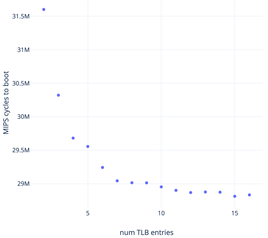
Most of the RAM usage by the emulator is non-negotiable. The MIPS register state will never be smaller than 32x 32-bit registers. The emulator state will never be smaller than the 96 bytes it occupies. However, the TLB can be variably-sized, as I mentioned above. So, in the interest of allowing some money to be saved in replicating this project, my code allows one to populate 1, 2, 3, or 4 chips in the 3rd RAM bank, producing a TLB of 4, 8, 12, or 16 entries. The chips in that bank need to be populated in-order, from left to right, so the options are 1 or 2 4002-1s, and if you have two populated, then you may also populate 0, 1, or 2 4002-2s. As expected, the performance scales inversely to the number of TLB entries. I should warn, however, that the 4002s that provide the TLB also provide the LED outputs for the high 16 bits of the PC display LEDs, so if you partially populate this RAM bank, some of the LEDs will not work.
A fun sidenote: the code actually will probe and support any TLB size from 1 to 16 entries. Each 4002 holds 4 entries so in the real world, only multiples of 4 are possible, but in the emulated world, anything is possible, so I tested every value between 2 (the minimum to boot) to 16. Here you can see a graph of the number of MIPS CPU cycles needed to boot to shell vs the number of emulated TLB entries. It is notable that while the difference from 4 entries to 8 is large, the difference from 12 to 16 is not, so populating just an 8-entry TLB might be enough. This can save you about $50 at current prices...
The prices for 1971 chips
Sadly, you'll still spend quite a bit of money buying the 1970s parts. Here I have a table of the necessary old chips, their various names, and my best guess as to how much you'll pay (as seen by me on eBay USA at the time of publication). Some parts were only available from intel, while others were also available from National Semiconductor. Parts annotated with (g) are ceramic with gold (usually white ceramic, most rare, most expensive), (c) are parts that are grey ceramic (also rare, also expensive), and parts with no annotations are plastic and are the cheapest (still expensive). All of the part numbers listed in each cell function identically so you can buy the cheapest. I also designed this board to accept either a 4004 or a 4040, so you only need to buy one of them, probably whichever is cheapest. I am unable to explain the price difference between 4002-1 and 4002-2, since they are basically the same chip.
| PART | USE | # NEEDED | Typical $ | NAMES |
|---|---|---|---|---|
| 4004 | CPU | 1 or 0 | $250 | C4004(g) D4004(c) P4004 INS4004D(g) INS4004J(c) |
| 4040 | CPU | 0 or 1 | $60 | C4040(g) D4040(c) P4040 |
| 4201 | CLOCK | 1 | $50 | C4201(g) D4201(c) P4201 INS4201J(c) INS4201N |
| 4002-1 | RAM 1 | 5 - 6 | $7 | C4002-1(g) D4002-1(c) P4002-1 INS4002-1D(g) INS4002-1J(c) INS4002-1N |
| 4002-2 | RAM 2 | 3 - 5 | $25 | C4002-2(g) D4002-2(c) P4002-2 INS4002-2D(g) INS4002-2J(c) INS4002-2N |
| 4289 | ROM CTL | 1 | $70 | C4289(g) D4289(c) P4289 |
It should be noted that the prices are so high because of "collectors" who buy up these CPUs with no intention of ever using them. To them, any 16-pin chip laser-engraved with "P4004" would do just fine, but they instead insist on buying real chips, denying their use for real projects! What a dick move! However, it gets worse. The chips with gold caps are also sought out by people who "harvest" gold from them. This is a euphemism for grinding them up, destroying them forever. Ugh!
The modern parts
The modern parts of this project are downright affordable in comparison. The one thing that might be hard to source is the SPI VFD, but they do show up on eBay often, and I got mine for $15 each. Alternatively, another SPI display can be used with small code changes. You can also just not populate the VFD at all and interact with the device over the serial port only - this is fully supported and works well.
I also added some cleverness around the SPI PSRAM usage. PSRAM chip count and size is auto-detected. The first PSRAM must be at least 4MB in size, since the kernel expects to be loaded contiguously there and it is 2.5MB in size. So populate a 4MB or an 8MB chip first. If you work at ISSI and have access to a pre-production 16MB chip, that will also work. The second PSRAM chip can be left unpopulated, or populated with any size chip you have. I tested everything from 128KB to 8MB. Keep in mind that while more RAM will help Linux run better, it will slow down the boot process slightly. Sizes under 128KB are unsupported.
Thanks to my work on minimizing the size of the Linux kernel by aggressively culling the kernel config, the kernel I provide is small enough that you can boot to a shell prompt without using swap on only 4.5MB of RAM (eg: a 4MB chip + 512KB chip). You may then enable swap and go on. Although, given the cost of 8MB PSRAM chips, I do not know why you'd do this other than just curiosity.
How it works
The connections
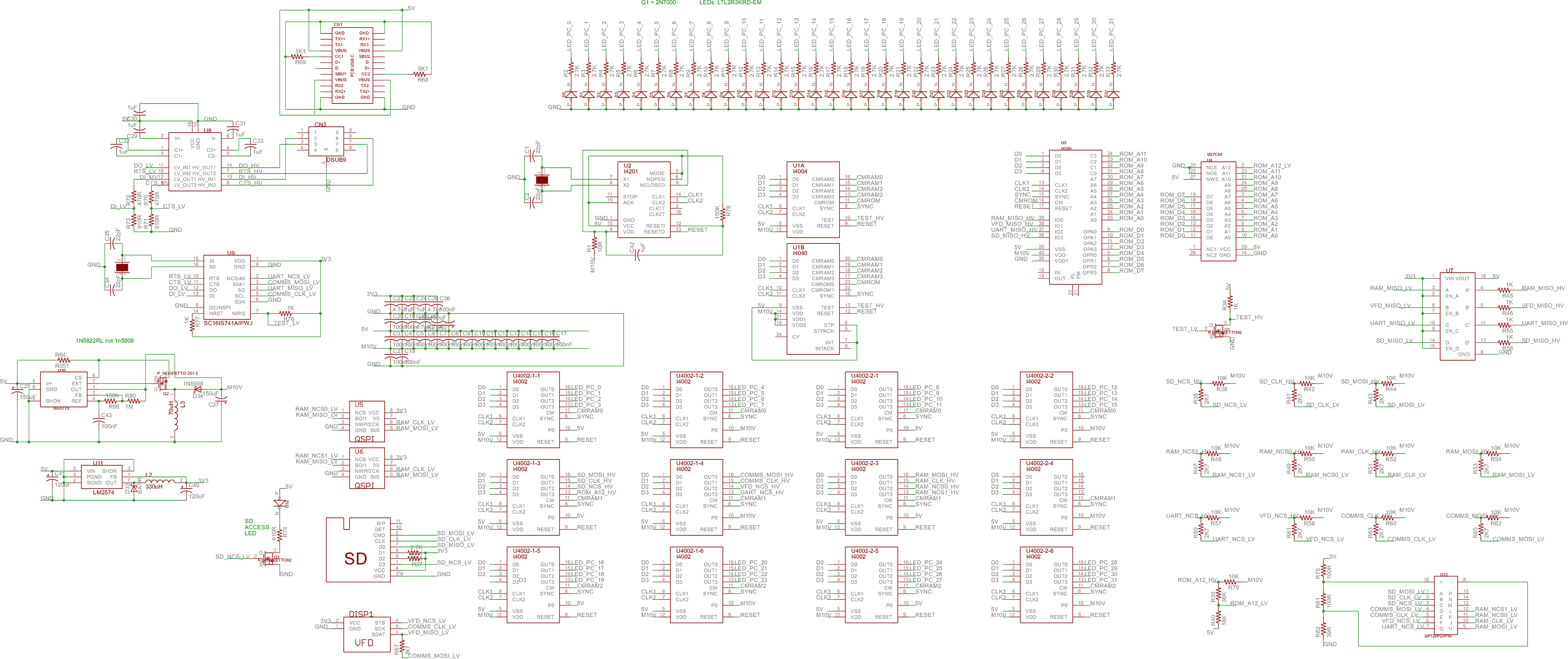
At a high level, ignoring all the level shifting messes, the board is pretty simple. The 4201 generates the clock and reset signal for all the components. An RC network generates the reset input signal for it. The 4002s in the first and third banks are connected to the PC LEDs, in the obvious order. The first bank provides the low 16 bits, the 3rd provides the high 16 bits. The second RAM bank provides all the outputs used for driving various SPI busses and the ROM bank selection, so any 4002 mentioned from now on in this section is a 4002 in the second RAM bank. This RAM bank is composed of three 4002s. Board space is provided for a fourth 4002 in this bank, if you want to use this board for some other reason, eg as a fancy 4004 dev board. The first 4002 in this bank is used for the SD card's SPI bus. In order, the output pins are: MOSI, CLK, and nCS. The last output pin acts as A12 to the ROM, flipping ROM between bank 0 and bank 1. The second 4002 is used for communications. Its outputs, in order, are: MOSI, CLK, VFD.nCS, UART.nCS. The third 4002 is used for the PSRAMs. Its outputs, in order, are: MOSI, CLK, RAM0.nCS, RAM1.nCS. The 4289 is connected to the lower 12 address lines of the ROM. Its inputs are, in order: PSRAM.MISO, VFD.MISO, UART.MISO, and SD.MISO. UART chip's IRQ line drives the TEST input on the 4004. That is basically it!
SD card access
What could be simpler, one would think, than accessing an SD card? The spec is rather clear on how to do that over SPI: three wires to the card, one back; send some commands to init it, then one command is for read and another is for write. Trivial, right? It might be for modern microcontrollers that have kilobytes of RAM. The Linux/4004 board has a total of 440 bytes of RAM, if you count the un-addressable status nibbles, 352 if you do not. Of them, 160 (or 128 if you do not count the status nibbles) are hard-allocated to virtual MIPS registers, and another 160 (or 128 if you do not count the status nibbles) are hard-allocated to the TLB. This leaves 120 (96) bytes of RAM left. This is not enough to talk to an SD card, since the minimum unit of reading or writing an SD card is a 512-byte sector (very old SD cards allowed partial-sector reads, but partial-sector writes were never a thing). Adding another full RAM bank would only add 128 addressable bytes. It would take 4 full banks to fit a single 512-byte sector. This would force me to use an external 3-to-8 decoder to allow the 4004 to address this much memory. Plus, those chips are expensive! And, I had sworn I would not do this. Another solution was needed.
Well, the SD card has its own SPI bus, as do the PSRAMs. The emulator itself never really needs to process SD sectors' contents, only place them into the virtual RAM or write them from the virtual RAM to card. So, the SD sector data can always be read directly into PSRAM, or from it. This will work nicely since they have separate SPI busses. As we read card data, every 4 bytes we read, we'll write to PSRAM at the requested address, and then increment it by 4. Repeat 128 times. Writes will work much the same way. Due to the slowness of the 4004, this process is hilariously slow. It takes a bit over a second to read or write a sector to the card. But at least no extra 4002s chips are needed!
Which brings us to a potential issue with SD card access. The SD spec specifies that to properly initialize an SD card, one needs to send ACMD41 at a clock rate of 100KHz - 400KHz, and at least once every 50ms. The SPI bit-banged out the output ports of a 4002 cannot meet either of those timings. I cannot even approach them. I had some concerns. They went away quickly. Every SD card I tested happily initialized even at 5KHz, with ACMD41 sent every 200ms or even more rarely. I guess this makes sense since modern SD cards do not use the provided clock for anything internal, like original ones might have considered doing.
How it boots
The firmware necessarily must know how many TLB entries there are, since it needs to prevent the virtual MIPS CPU from populating the INDEX register with a higher value, and it needs to make sure that the RANDOM register also never presents a higher value. The firmware, thus, starts by probing the number of memory chips in the third bank, to then figure out how many TLB entries there are. Then, the VFD and the UART chip are initialized, then the SD card is initialized. If this fails, a message is shown: "Failed to init SD card. Halting here and now!". This message is the only string in the entire firmware, since bytes in this ROM are worth their weight in gold!
Every byte in the firmware has a high cost due to the very limited nature of how many bytes of ROM the 4004 can address. Additionally, having a virtual ROM requires an extra check in the decoding code for every memory access. No, it is not worth it to have a virtual ROM like the real DECstation 2100 had. Instead, my firmware simply loads the first SD card sector to the beginning of RAM (0x80000000), and then jumps to there. The code there is, as you'd expect, limited to 446 bytes that there is before the partition table starts. The code reads the partition table (which is also in RAM, as it is part of the first SD sector), finds a partition with type 0xBB, and reads it, in its entirety, to RAM at 0x80001000. If this goes well, it jumps there. If the partition is not found or the reads fail, a short message is shown using a trivial function that can output a string to the console using a hypercall to print each character.
This second loader can be arbitrarily large (mine is about 14KB) and can be written in C. When there is this much space, you get some creature comforts, like real printf() with formatting. I mostly reused the loader from the LinuxCard project, but with some adjustment and simplification. When every cycle counts, one seeks to reduce the number of cycles used. I simplified and prettyified the progress bars and removed zeroing of the .bss, since the kernel will do it itself.
Some things, however, had to be added. The RAM size probing is done here now instead of in the emulator itself. This saves space in the emulator firmware. The emulator treats each of the two RAM windows (0x80000000 and 0x82000000) as being 16MB in size always. It counts on Linux to only use the RAM that really exists. But how would Linux know? It asks the bootloader using the REX API. How does the bootloader know? It probes the RAM and notes the sizes of each one. The loader also probes the TLB entry count (by writing incrementing values to the INDEX register and seeing when the write does not take, as the emulator limits writes to valid values). This does not need to be communicated to Linux, as it does not care. But it is nice to know, so it is printed onscreen.
Eventually, the loader finds the partition marked as active, mounts it as a FAT12/16/32 filesystem, finds a file called vmlinux on it, parses it as an ELF file, loads it to RAM if it is valid, and jumps to its entrypoint, giving it the proper parameters of machine type, a magic value, and a table of callbacks into "ROM" for things like RAM mapping and early console printing. If any part of this fails, a descriptive message is shown onscreen.
As a small improvement, to save time on busyloop calibration, I ran it once, recorded the value, and now provide it via the kernel command line. This saves noticeable time every boot.
How it runs
Disk access, same as in LinuxCard, is provided by the PVD paravirtualized disk driver. This is much simpler than attempting to emulate the SII SCSI chip and a SCSI disk in 4004 assembly. The hypercall to read or write a sector acts like DMA to the virtual MIPS machine, completing instantly and delivering data to virtual RAM or taking it from virtual RAM. The driver is completely unmodified from its state in LinuxCard.
As virtual timer interrupt ticks at 16Hz, and and IRQ is delivered to the virtual CPU every 65,536 virtual instructions, the virtual CPU thinks it is running at 1.05MHz. My testing shows that the actual emulated speed of the MIPS guest is around 70Hz at 740KHz. I run the 4004 at 790KHz, so the emulated guest is thus operating at about 74.73Hz. So time for the guest is dilated by 14,030x. This means that a virtual second is, in real life, around 3h54. Four hours per virtual second, basically!
The power consumption is around 6W, so any PD-compliant USB-C brick capable of supplying 2A @ 5V will do. The LED next to the SD card is a combination power/activity light. Since the guest CPU is so slow, even very active SD card usage is very low duty cycle. Thus, mostly the SD card will be idle. This fact is used to make a combined indicator light. It will be on while the board is on, and go off for about a second for every SD card sector read.
The art of it
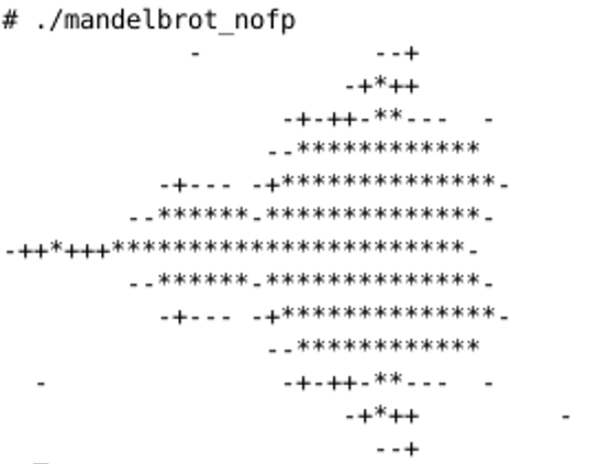
The goal of this project was always partially artistic. This is why the board has a pretty VFD on it, why I designed it to look retro, and why it has hanging holes on the top corners! The idea is that, once completed, it can be hung on a wall where it will slowly do ... something. What could that something be? Well, I wrote a simple program that draws (in text mode) the mandelbrot set on the VFD (and on serial port). There are two versions: one uses floating point numbers (/root/mandelbrot in my image), which Linux ends up having to emulate, which makes it slow - around 30 days to draw the entire 13 rows x 40 cols image. The second version is integer-only (/root/mandelbrot_nofp in my image). That one completes in under 9 hours. But for the one I'll have hanging in my office, I have loftier goals. With swap enabled, the kernel sources can actually be built right on-device. It will take some number of years. The partition where the kernel lives is /dev/pvd2 and is mounted under /boot. The device can build its own kernel from source, copy it to /boot/vmlinux, and reboot into it. If power is interrupted, thanks to ext4, it will reboot, recover the filesystem damage from the journal, and restart the compilation process. That is my plan, at least.
I want one
Build one
The schematics are above, and the BOM of modern components is as follows. The table earlier summarizes the 1970s components needed. You can build one relatively easily.
| WHAT | COUNT | VALUES | NOTES |
|---|---|---|---|
| IC-16 | 11 | 16-DIP socket for old chips | only for the MCS-04 parts |
| IC-24 | 1 | 24-DIP socket for 4040 | Only if you want to use a 4040 |
| IC-28 | 1 | 28-DIP socket | for the ROM |
| IC-40 | 1 | 40-DIP socket | for the 4289 |
| EEPROM | 1 | AT28C64B | Unless you have a 8Kx8 EPROM already |
| U5, U6 | 1 or 2 | AP Memory 2MB PSRAM, AP Memory 8MB PSRAM, ISSI 128KB SRAM, ISSI 512KB SRAM, ISSI 1MB PSRAM, ISSI 2MB PSRAM, ISSI 4MB PSRAM, ISSI 8MB PSRAM, Microchip 256K SRAM, Microchip 512K SRAM, Vilsion 8MB PSRAM | RAM1 (U5) must be 4MB+, RAM2 (U6) can be any size >= 128K |
| U7 | 1 | CD40109B | or equivalent |
| U8 | 1 | HIN232 | or equivalent |
| U9 | 1 | SC16IS741A | |
| U10 | 1 | MAX774EPA+ | |
| U11 | 1 | LM2574-3.3YN | or equivalent |
| U12 | 1 | SP720APP | or equivalent |
| CN2 | 1 | Dsub 9pin male connector | |
| CN3 | 1 | SD-4-B SD card connector | |
| L2 | 1 | 330uH 800mA inductor | |
| L3 | 1 | 40uH 3A inductor | strongly suggest using this one |
| D0, D1, D2, D3, D4, D5, D6, D7, D8, D9, D10, D11, D12, D13, D14, D15, D16, D17, D18, D19, D20, D21, D22, D23, D24, D25, D26, D27, D28, D29, D30, D31, D32 | 33 | 3mm LED | |
| D33 | 1 | 1A Schottky Diode | strongly suggest using this one |
| D34 | 1 | 3A Schottky Diode | strongly suggest using this one |
| X1 | 1 | 5.5296MHz MHz XTAL | Or you can use another of similar freq |
| X2 | 1 | 3.072MHz MHz XTAL | Or you can use another of the same exact freq |
| Q1, Q3 | 2 | 2N7000 | Or another similar N-FET |
| Q2 | 1 | IRFU5305PBF | or equivalent |
| R2, R3, R4, R5, R6, R7, R8, R9, R10, R11, R12, R13, R14, R15, R16, R17, R18, R19, R20, R21, R22, R23, R24, R25, R26, R27, R28, R29, R30, R31, R32, R33, R35, R36, R37, R41, R43, R47, R49, R51, R53, R59, R61, R63, R65, R67 | 46 | 2K7 1/8W resistor | |
| R38, R42, R44, R48, R50, R52, R54, R57, R58, R60, R62, R79 | 12 | 10K 1/8W resistor | |
| R34, R45, R46, R55, R56, R76, R77 | 7 | 10K 1/8W resistor | |
| R71, R73, R74 | 3 | 910R 1/8W resistor | |
| R75, R81 | 2 | 100R 1/8W resistor | |
| R66, R78 | 2 | 150K 1/8W resistor | |
| R70, R72 | 2 | 470R 1/8W resistor | |
| R68, R69 | 2 | 5K1 1/8W resistor | |
| R1 | 1 | 10R 1/8W resistor | |
| R40 | 1 | 18K 1/8W resistor | |
| R80 | 1 | 1M 1/8W resistor | |
| R39 | 1 | 36K 1/8W resistor | |
| R82 | 1 | 39R 1/8W resistor | |
| R64 | 1 | R051 resistor | or equivalent |
| C3, C4, C5, C6, C7, C8, C9, C10, C11, C12, C13, C14, C15, C16, C17, C18, C19, C20, C21, C36, C43 | 21 | 0.1uF decoupling cap | |
| C23, C24, C29, C30, C31, C32, C33, C42 | 8 | 1.0uF cap | |
| C25, C37, C38, C39 | 4 | 150uF 25V low-ESR cap | strongly suggest using this one |
| C1, C2, C34, C35 | 4 | 22pF cap | |
| C22, C26, C27, C28 | 4 | 4.7uF cap | |
| C40, C41 | 2 | 120uF 16V cap |
Kit or pre-built
I am considering offering this as a kit. You'd get the board and all modern parts labeled and ready to assemble. Other than the three surface mount parts, all others are very large through-hole components that anyone can assemble trivially. The PSRAMs are also quite easy to solder down as they only have 8 pins with large spacing. If you are interested, write to me at kit4004@dmitry.gr. I might offer a kit that also includes the 1970s components. The price on that one will mainly depend on the costs of acquiring the old chips.
I do have enough components to build a few fully-working boards, tested and with all the chips. If you REALLY want one and do not want to do any work assembling one, write to me at full4004@dmitry.gr and we can discuss. It will not be cheap, as you can guess.
Making of the video
This was an adventure enough to warrant its own section
Capturing
Of course, this was not going to be easy, but I must admit that I severely underestimated how difficult this would end up being. The idea was simple: set up a phone to take a photo every second or so, collect the photos, make a video. Done. Right? Let's do some math. A 1920x1080 photo is around a megabyte in size. Taking a photo every two seconds generates around 1.76GB of data per hour. The filming took 9 days, which is 216 hours. It will, thus, produce around 379GB of photos in approximately 388 thousand files. I guess I'll need to come and offload all the photos from the device a few times to keep it from filling. Annoying but doable. Let's try!
I initially tried to use an old Pixel 5. I used an app that takes a shot every second as a test to see how well it would go. The device hard-hung overnight. I tried again, it did again. OK... I tried an older Pixel 3 XL. In the morning it was hung and too hot to touch. I am happy that the battery did not explode, having been heated that much. I gave up on android devices at around this point. The next candidate, logically, was an iPhone. I had an iPhone SE3 around that I strapped into the tripod to test. On iOS there was no free program I could find to do a timed capture with no shot limit, so I was forced to buy this one. It is quite annoying to have to buy an app whose sole function is one library function call a second and a sleep(), but this was faster than digging up Xcode and writing it myself. Overnight, the iPhone stayed functional. In the morning it was still taking photos and was not even warm to the touch. A tip of my hat to Apple engineers!
The actual filming was slow, as expected. I set up a video camera so I could watch remotely and know when to come to enter the next command. I did mess up once, however. When I entered the uname -a command, I did not press ENTER. I only realized that later - next afternoon when I noted that the cursor was still on the previous line. I came over and pressed it then, but this added 9 hours of nothingness to the video.
Getting the data
Said hat tip was soon rescinded. SE3 does not have the storage to capture all the photos. I had planned to offload the data once a day using either the "Photos" app or the "Image Capture" app on a connected MacBook. After about two such offloads, Photos app stopped seeing new photos in device memory. I tried re-plugging USB and restarting the MacBook. Neither worked. Restarting the phone did, but of course this creates a gap in the recording and is unacceptable. Image Capture seemed to work better. It could copy photos off and delete them from the device, freeing space. Good! After three such offloads, the "delete" functionality stopped working. It could still copy new photos from the device but it refused to delete any. Again, the only thing that helped was restarting the phone. Again, this is unacceptable.
I tried a few more times, wasting a few more days, with no better luck. I gave up and grabbed an old 512GB iPhone 12 Pro Max with a shattered screen, shelled out $130 to have it replaced with the cheapest third-party display, and strapped it into the tripod. I decided to just capture everything nonstop and grab the photos later. This should have allowed me to skip the bugs in Photos and Image Capture apps.
Final photos taken, it was time to grab the images from the phone and stitch them into a video. This did not go well. Photos app only saw around 100,000 of them. The number differed every time I plugged the device in, but never rose to the correct number around 400,000. If I tried to tell it to import anyways, it hung. Leaving it alone for a day produced no results. Image Capture had a similar issue, although once it saw around 200,000 photos - a number that Photos never got up to. If told to import, it would say "Importing FILENAME.JPG" and stop there, having created a zero-sized file with the given name in the target directory.
OK, I can try to make a local backup of the iPhone to a MacBook, then decrypt the archive and get photos out, right? The backup button in Finder worked. As expected, the iPhone asked for the pincode to authorize the backup. The progress bar showed the moving cross-hatched pattern... a day later no progress had been made. Maybe AirDrop will work? Well, first of all, there is no way to select all photos in the Photos app (still) without dragging your finger across them all. You have no idea how long this takes for 400,000 photos, especially as the app gets slower and laggier as you go on. Somehow there is no "select all" option. I lost patience at 20,000 photos selected and decided to try to AirDrop those, then select more. The Photos app crashed trying to AirDrop this many photos. I tried with 10,000 and it crashed again.
Fine! I'll give up and use the cloud. I installed Google Photos and told it to backup to my account. It took over an hour "preparing to sync". It then synchronized around a hundred photos and promptly crashed. Opening it again produced the same result - over an hour of preparation, and another 100 photos got uploaded. This was not sustainable, neither in rate nor in manual labour required to keep re-opening the app. Unlike Apple's Photos, Google Photos DOES allow easy multi-select. With one tap I was able to select all photos taken on a given "Tuesday" and click the "Back up" icon. The app promptly crashed.
In frustration, I paid Apple for 2TB of iCloud, figuring that the cost of one month of it is fine to resolve my growing frustration. No crashes, and it started syncing. The sync speed hovered at around one photo every 5 seconds. My internet connection has 1 Gbit/s upload so it was not that problem. This was going to take forever!
Getting desperate
Maybe Windows could do better? I plugged the iPhone into my ThinkPad running Win10x64. It is supposed to show up in "My Computer" and have a DCIM directory with photos in it. It did the former, but not the latter. Googling around indicates that this is common - iPhone asks for pincode to confirm trusting the PC, and then nothing still. The typical "solutions" include "try cleaning your registry" and other such idiocy. OK... I guess it is Linux time? My Thinkpad had an install of Linux Mint 18 on it. It saw the iPhone but also saw no photos on it. Googling around indicated that some work had been done rather recently on iPhone <-> Linux comms, and a tool called ifuse can successfully mount an iPhone using FUSE. The version in Linux Mint 18 was too old to work, of course. It failed with incomprehensible errors, and panicked my kernel once.
In the typical "it is called open source because you have to open the source to get anything at all to work" fashion, I had to download it and build it from source. Some dependencies were also too old, so I had to build them. Eventually, after much googling, building, installing, and cursing, all the things were built and it was time to try them. idevicepair successfully paired to the device. ifuse mounted the device at a given mountpoint, and there was indeed a non-empty DCIM directory in there! Success! I'll just drag that over to my desktop and be done, right? Well, that hung. I guess the Nautilus file manager was not prepared for such large copies. Maybe it tried to stat() each file or maybe it has some O(n^3) algorithms in there. I do not know. I re-plugged the iPhone, re-mounted it, and used good old cp -Rvf to copy all 400,000 files uneventfully ... over 10 hours.
Making the video
Dealing with this many files was annoying in a number of ways, and the sole working solution was almost always some soft of a CLI utility or script. After getting all the files out, they had to be renamed to sequential names. I did not dare mess with my hard-gotten source material, so instead they were copied with new names. A file list, vim, and one very gnarly regex later, a command list was created to do the copies. The copying took a little over 3 hours. I am not sure if I should blame ext4, md-raid, or myself for this...
I have never used any video editing apps, and I saw no reason to start now. A series of very messy ffmpeg commands were used to create the title screens, add the music to the first, create the video from the photos, and combine them all together into the final video. There is no time missing in the final video, but the playback speed is variable to speed up the boring bits. There is a clock and a calendar visible onscreen so you can easily see the time elapsed. Playback speed varies between 5FPS (10x realtime) and 960FPS (1920x realtime) to keep the video short(ish) and to-the-point(ish). It is hilarious that at some points in time you can see the changing of day to night and back by the light shining onto the table from the window (out of frame to the right). Due to the speed-up used, you may miss the blinking of the SD activity light (though you can see it blink a few times as the rootfs is being mounted and later as ls executes). Sorry. However, if you really want to see it, see next paragraph.
For those who like raw data, do not trust my edits, or just want to see it at a constant speed, I also produced a completely unedited version of the video, which you can see here. As the capturing was done at 0.5FPS and the playback in this video is at 60FPS, the video is sped up 120x from realtime. As 4 hours of realtime map to one second of emulated time, and the video is 120x faster than realtime, 2 minutes of video map to one second of emulated MIPS processor time.
Downloads
The disk image for the SD card can be downloaded here (mirrored here). It is a separate download due to its size. The main download is here. It contains the MCS-04 bus analyzer for Saleae software, source code for the i4004 Dectstation2100 emulator, source code for the MIPS MBR and second stage bootloaders, kernel config and version info, as well as my very-scary u4004 emulator of the Linux/4004 board. License is: free for non-commercial use. Commercial use requires a license, contact me for licensing. Any use must credit me in source and binary form.
Credits
Much thanks, as usual, to my cats for cutely sitting near my feet as I worked on this, Eric (TubeTimeUS) for bravely loaning me some MCS-04 chips before I could acquire my own, eBay for occasionally supplying good deals on old chips, and M @ Entropic for helping me fix my shitty switch-mode -10V supply. This time, the mount-rushmore-sized middle finger goes out to MCS-04 "collectors" who gobble up the supply at insane prices with no intention to ever use them. My offer to you, miscreants, is simple: I will trade you any working MCS-04 chip you have for a very pretty PDIP-16/24/40 that I will have laser-engraved with the same exact label. Nobody who "sees" your collection will ever know, and the world will gain another MCS-04 chip that might actually be used!
Comments...
