An interactive-speed Linux computer on a tiny board you can easily build with only 3 8-pin chips
TL;DR
I've long been experimenting with minimal computers that can run Linux. I've flirted with the extreme low-end and with fun form factors. I felt like there was a place for another fun experiment: a simple-to-build kit computer using only 8-pin chips.
Table of Contents
- A minimal computer
- Designing the hardware
- The software story
- Performance
- Assembly
- Downloads and Use
- Comments...
A minimal computer
Initial Thoughts
There was a time when one could order a kit and assemble a computer at home. It would do just about what a contemporary store-bought computer could do. This time is long gone. Modern computers are made of hundreds of huge complex chips, with no public datasheets, with many hundreds of watts of power supplied to them over complex power delivery topologies. It does not help that modern operating systems require gigabytes of RAM, terabytes of storage, and always-on internet connectivity to properly spy on you. But, what if one tried to fit a modern computer into a kit that one could easily assemble at home?
What is the minimum to be considered a "modern computer"? I would say being able to run Debian Linux, vi, gcc, and make is close enough, so that became the goal. Thanks to my previous exploits, I knew that this could be accomplished in 8MB of RAM and with 1 MIPS of CPU. Storage is easy: SD cards easily provide storage of any size. A serial port is still the de-facto method for easily interfacing with an embedded system, but as computers no longer have serial ports, USB-serial takes its place. Thus, I had the target: at least 8MB of RAM, at least 1 MIPS of CPU, SD card, USB.
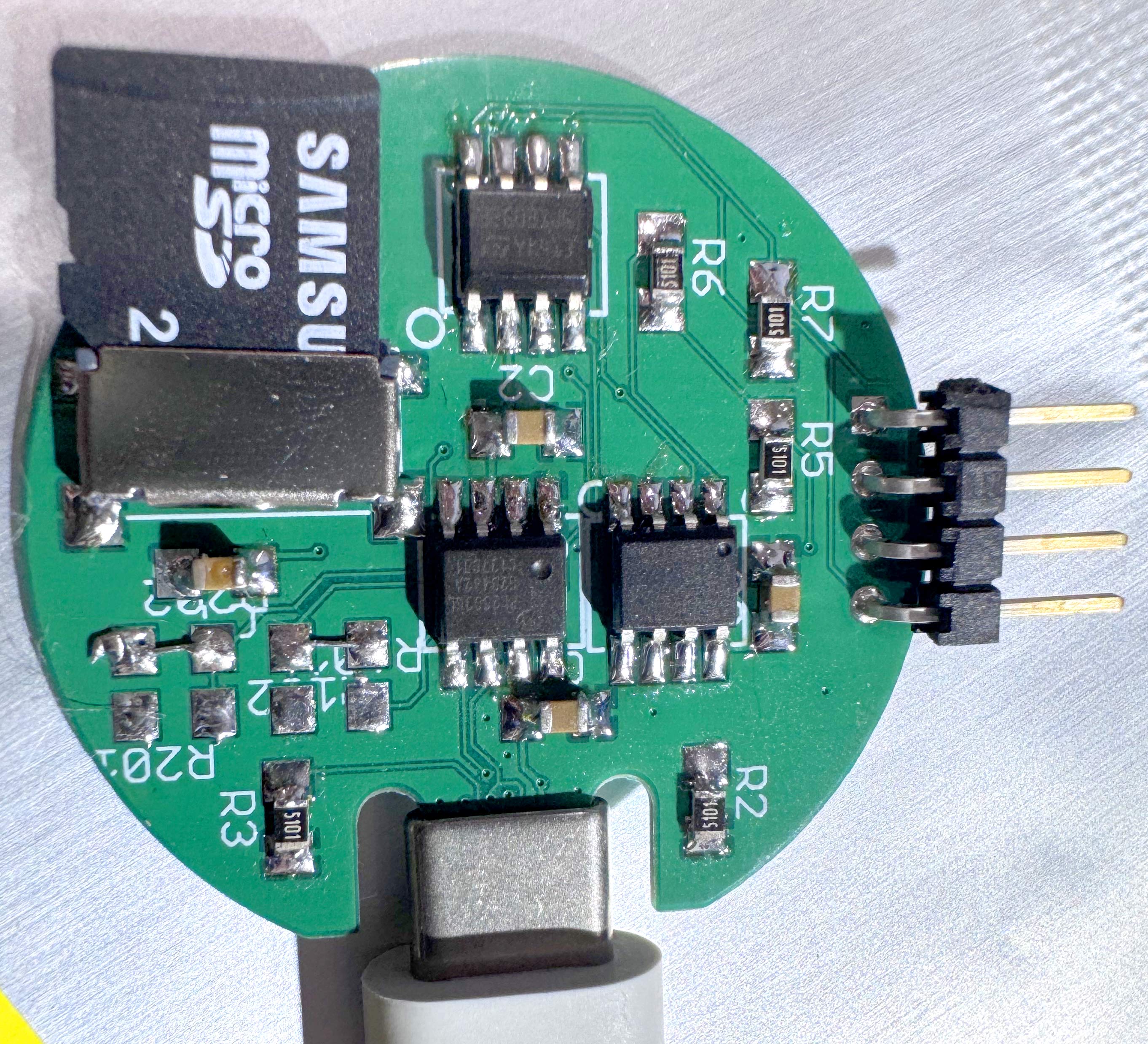
On the hardware front, I wanted to design something that could be assembled by someone with little-to-no soldering experience and a RadioShack 45W soldering iron, something small, cute, and cheap. Chips with fewer pins are easier to solder, so I settled on using only chips with 8 pins, as a fun challenge. Since all chips need at least a power supply and a ground pin, this limits each chip to no more than 6 useful pins. This decision turned out to inform a lot of the design's features and limitations. Physically, I decided to make it a small circular board, with a board-edge USB-C connector on top, as you can see on the image here. That is the final working design, assembled using the directions below, by me, actually using a RadioShack 45W soldering iron.
Parts Selection
There really are not too many 8-pin chips that can speak USB. One and a half options exist. The first was the very cute PL2303GL, which is a USB-to-serial bridge that requires NO external components at all, and even provides 100mA of 3.3V regulated output. Super convenient! It works precisely as promised. I am a fan! Prolific even have drivers for all major and minor operating systems available easily. Sadly, on macOS, they need to be installed from the AppStore, but it is a simple process. It should be noted that its predecessor, the PL2303SA could also be considered, but it is EOL, and thus not worth mentioning. So, what is meant by "half a chip"? Well, thanks to V-USB, The ATTINYx5 series chips can also speak USB. It is only USB low-speed, and uses a lot of CPU time, but it works. The problem is that all existing USB-serial protocols require bulk endpoints, and USB low-speed is prohibited by the USB spec from using BULK endpoints. To stay spec-compliant this would then require designing my own comms protocol using interrupt endpoints and writing drivers for all major OSs. No fun. Luckily, ALL major OSs do not enforce this no-bulk-EPs-on-USB-low-speed thing. It just works, and implementing ACM to act as a serial port works. So, there they are - the two options for USB interfacing.
There were not really any questions with regards to the RAM to use. SOIC-8 PSRAMs are the solution. ISSI, APMEMORY, and Vilsion make them. All of them have been promising 16MB chips for a year now, and none have delivered, so it is probably fair to assume that they are all bullshitting. However, 8MB parts are easily available for a few bucks at the usual retailers, so it was decided to make it work with 8MB of RAM.
The last question was: which microcontroller to use? A parametric search presented a few families of options:
- PIC16F is a messy old 8-bit architecture that can really only be programmed well in assembly. There is a C compiler, but it produces shit code (not its fault - the architecture is not well suited for C). These clock up to 32MHz, but as they take 4 cycles per instruction, the real performance is 8MIPS at 8 bits per op at best. The fact that this is an accumulator-based arch means that most things take more instructions. Overall, not a performant option. The largest code space available is 8192 instructions' worth (14KB), and the largest RAM available is 1KB.
- Renesas R5F series is a weird little 16-bit core they call RL78. There is a passable GCC port for it too. The instructions take a variable number of cycles between 1 and 6. For typical code it'll average an IPC of 0.55, and at 16MHz at most. They do not overclock well either. At least these cores are 16 bits wide, so they can do more per cycle than the PIC. In the 8-pin package, the largest possible flash size is 8KB. RAM? 1KB. As instructions are all at least 2 bytes, this option is limited to 4096 instructions at best, possibly less. It would be fair to expect 8MIPS at 16 bits per op.
- PSoC1 series uses a core Infineon (née Cypress) calls M8C. Instruction encoding is pretty dense, with many instructions being only a byte long. Sadly, the performance is not there. No instruction takes fewer than 4 cycles, and some take over 10 cycles, including function calls. The maximum clock rate is 24MHz, with overclocks of 28MHz possible. But at an average of 6 cycles per instruction in a typical program, this only nets ~4.7MIPS at 8 bits per op. Not great. The maximum flash size is 4KB, and RAM is only 256 bytes. This is ... not great.
- Somehow, ZiLOG still exists, and they sell 8-pin microcontrollers based on the core they call eZ8. In the 8-pin package, the maximum flash size is 8KB, and RAM is 1KB. The core seems to use variable-length instructions, but they are quite slow. Most seem to take 2-4 cycles to fetch and then 3 or more to execute. Jumps take a lot more. Overall, expecting this core to get an IPC of over 0.2 is probably asking for too much. The maximum clock rate for these microcontrollers is 20Hz, so that should be about 4 MIPS at 8 bits per op. A new low.
- NXP's S08CPUv2 core makes an appearance in a few chips here. It is an 8-bit accumulator-based architecture that clocks up to 40MHz. The maximum flash is 8KB, RAM size is 512 bytes - tight. Instructions are 1-4 bytes long. While some of them execute in 1 cycle, most take 2 or more. My guess at this thing's IPC in typical scenarios would be 0.6 or so. It is 8-bits wide. Expected perf is thus around 24MIPS at 8 bits per op.
- STM8-based chips are an option. They are 8-bits-wide, run at 16MHz, have a pretty compact instruction encoding, and feature very high IPCs near 0.8, if you are lucky and keep the prefetch queue full. There is a C compiler available for these, too. In the 8-pin package, the maximum amount of flash is 8KB, and 1.5KB of RAM. Expected perf is around 13MIPS at 8 bits per op.
- MSP430 (aka: the 2000s' PDP11) is represented in the search results too. Sadly, with only 2KB of flash and 128bytes of RAM, none of these chips are of much use for this project - they are simply too tiny.
- There is, of course, AVR: 20MHz at 1.0 IPC, overclockable to around 25MHz easily, 8KB of flash and 512 bytes of RAM in the ATTINY85. There is an active GCC port, and the instructions are designed in the modern day and age, producing very compact and efficient code, none of that "move things into accumulator, now move them out of the accumulator" nonsense. This is the best option so far. As an extra bonus, if used for USB, then the entire board could be just two chips: the AVR for USB and CPU, and the RAM chip for RAM. Tempting. However, as V-USB needs about 1.5KB of flash and a hundred bytes of RAM, that leaves rather little to the emulator. It likely would not easily fit.
- My old friend, the PSoC4 is also represented in the results. A 16MHz ARM Cortex-M0 core basically obliterates all of the above options on performance trivially. It will execute most instructions in a single cycle (but branches take 3) and it is 32-bits wide. Flash size is 8KB officially, but, as I had documented, really there is 16KB. RAM really is just 2KB in size. The major downfall of this option is that it uses three pins for supplying power to the chip, leaving only 5 pins available for I/O. Being already short on pins, giving one up is a lot to ask!
- TI's new MSPM0C series is a possibility. The Cortex-M0+ core is even faster than a Cortex-M0 by virtue of taking one cycle fewer to branch. In an emulator this matters! 16KB of flash, 1KB of RAM, and all 6 pins usable as I/O. What's not to like? Well, one pin is open-drain only, which sucks. This makes the pin unsuitable for fast output. The speed is 24MHz, with a little bit of overclockability available. However, without a PLL, this chip cannot overclock far. Still, this is now the best option, easily outperforming the AVR.
- CH32V003, while not available easily from western sources, does come in a 8-pin package. A 32-bit CPU with 2K of ram, 16K of flash, and at 48MHz. It is passable, but I am allergic to RISC-V for personal reasons. An acceptable last-resort part, however
- The newer CH570E, from the same company as the above, is a curiousity. Faster than the CH32V003, more RAM and flash, USB, wireless. Cute, but.... the 8-pin part lacks USB support, lacks wireless support, and only has 3 I/O pins. what a joke!
- The last option (as using STM's chips should always be the last option due to their habit of not publishing accurate and complete errata sheets) is the STM32G0 series. The STM32G030 is immediately discarded as an option, since one of the pins is a permanent RESET input, leaving only 5 I/Os. The STM32G031J4M6 seems like a possibility. It is a relatively recent chip, so there is hope that STM got their shit together and fixed some of the usual myriad of issues their chips contain. Then again, as the plan called for minimal use of on-chip peripherals, maybe it'll be fine? 32KB of flash, 8KB of RAM! Those are serious numbers, completely obliterating the previous contestants. The Cortex-M0+ core makes it a tie for the best so far. Officially, this chip clocks at 64MHz. With effort, it'll overclock to 80MHz. With more effort (see below), it'll run at 150MHz. Assuming one can avoid the errata, this seems like the clear winner by far, as much as I hate it. Maybe one day there'll be an RP2354 in an SOIC-8 package with 6 PIO pins?
Designing the hardware
The Console
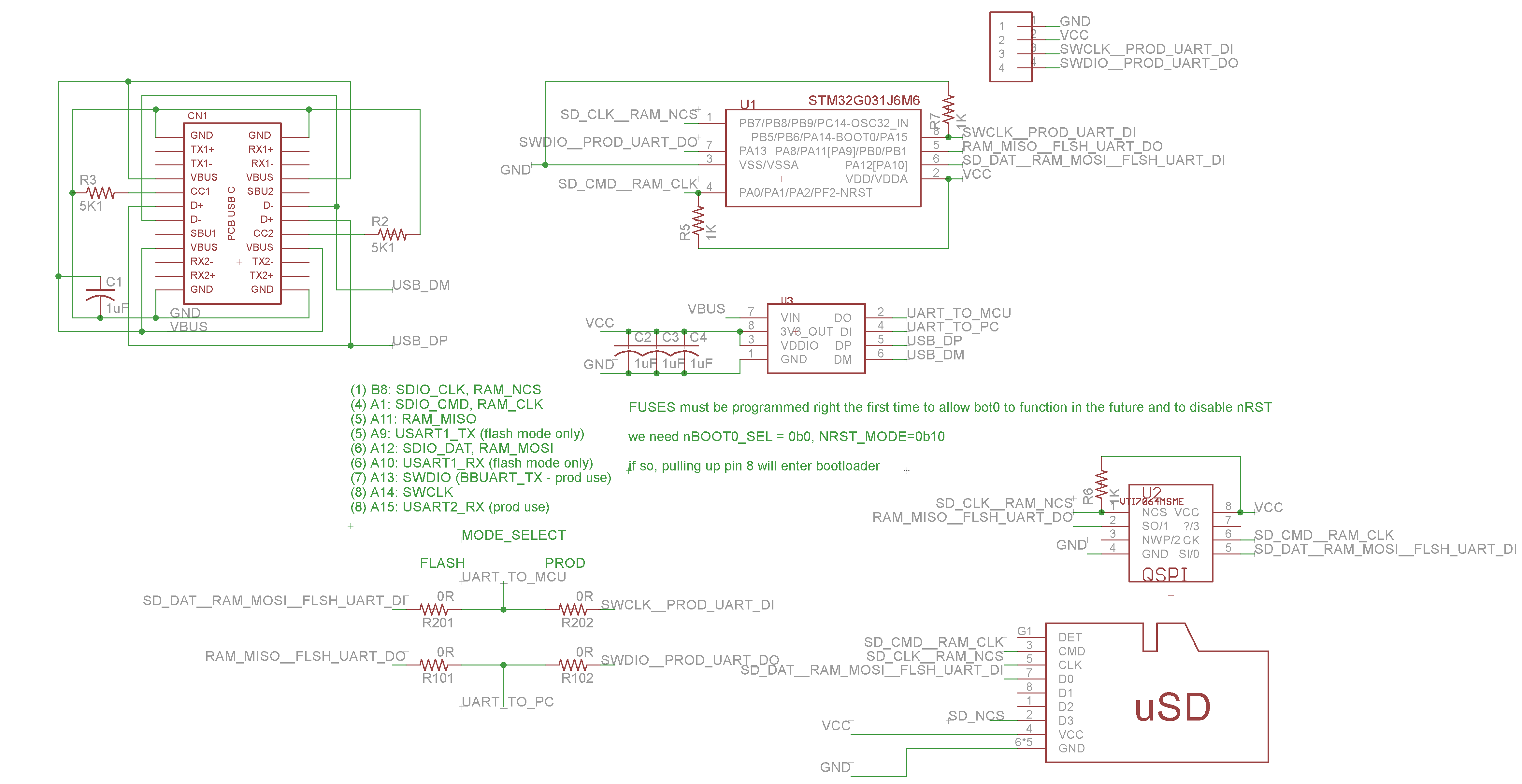
The UART pins cannot be combined with anything. Any attempts to combine UART RX with something would create the possibility of missing some incoming data while the "something" is going on. Combining UART TX with something, no matter how fast that "something" is, is problematic as well. Any low pulse would be seen as a character by the PC. For brief lows it would be seen as a 0xFF byte. In theory, parity could be enabled and used to hide this, but this is not surefire. Plus, who uses parity in 2024? Really, UART pins, lacking a higher-level protocol, chip select, or a separate clock are basically un-combinable with anything else. There go two of the 6 pins. Oh well...
RAM
All the SPI PSRAMS support QSPI mode for speed. Sadly, QSPI requires 6 pins and only 4 are left. OK, most of them also support dual-SPI, wherein MISO and MOSI are used concurrently to send two bits of data per clock unidirectionally. This is twice the speed of normal SPI, just as you'd imagine. As an extra credit, it does not require any more pins than normal SPI and is compatible with sharing the SPI bus with other devices, since they would not expect to read MOSI or drive MISO when deselected.
STM32G031 does not support dual-SPI. It could be bit-banged, of course. But, could it be done fast enough to beat the hardware SPI unit? The hardware SPI unit can run at one-half of the CPU clock and mate to the DMA unit for nonstop transmission/reception. To match this via CPU, would require bit-banging dual-SPI using no more than 4 cycles per clock. This is barely possible, given a few preparatory steps. Doing it any faster than that is impossible. Since the best that can be done is to match the hardware SPI unit, why bother? RAM will be accessed using garden-variety SPI. That uses four of the remaining four pins. Damn...
SD Card
So, here was the situation: no pins left and still an SD card to attach. SD cards speak SPI, so one more pin to give it a chip select signal would be enough, but there were no pins left. A few options were considered. The simplest idea was to include an inverter on the RAM's nCS and use that as the SD card's nCS. This was prototyped and it worked somewhat well. The issue with this approach is two-fold. First of all, some cards did not like being selected and deselected with no data bytes being sent to them, but that is precisely what two RAM accesses would look like to them. Not many cards had this issue, so it is not a showstopper. The second issue is that the inverter is either an extra IC or an extra transistor. The more components the board has, the harder it is for a novice to assemble. This solution was put aside, labeled "worst case". A search of a better one went on.
This device will not produce data very quickly, so it is safe to run the UART super slowly. So, then the UART TX pin can be low-pass-filtered on the way to the USB-to-serial chip. That same pin can then be used for SD card's nCS, as long as the commands are short and the clock rate is high enough that the selection time is below what the low-pass filter will permit through. This solution is workable but fragile. Once the math is worked out for the baudrate necessary to permit card initialization as per spec, it gets sadder. The UART would need to be run at a 300 bps rate or slower to make this work. And even then, it is fragile if the card decides to be slow, since the SD spec's SPI chapter does not technically allow deselecting the card while waiting for it to read data. No, this was even worse than the first option.
Before surrendering to the first option, there was a crazier yet option to consider. Would the SPI RAM at all mind being selected and then deselected with no commands or data in between? Experimentation provides the answer: no. This test passed on all the SPI RAM chips. Why? Well, besides SPI, SD cards also speak the SDIO protocol. Instead of using four unidirectional wires, this protocol uses one unidirectional CLK signal and two bidirectional signals: CMD and DAT. The four-bit-wide version uses three more data pins, but that does not matter here. Unlike SPI, this protocol is not quite documented in the public SD documentation, but it is not too hard to figure out. Using one fewer pins is nice, but there were no free pins, and this approach would have needed three, so this was not immediately useful. Before trying to make it useful, it had to first be make to work at all. After some time, this was done and a working implementation of SDIO 1-bit protocol was produced. It successfully initialized and accessed all SD cards tried. Cool.
So, which pins could be combined with SDIO's three? After much thinking, the solution is obvious. RAM's nCS can be the SD card's CLK. RAM's CLK can be the SD card's CMD. RAM's MOSI can be the SD card's DAT. Try and figure out all the possible interactions with each device and what that would look like to the other, to convince yourself that it will work safely. When the RAM is selected, the SD card will see its CLK go down, when RAM is deselected, the SD card will see its CLK go up. The RAM's SPI is configured for mode 3, which means that its CLK idles high. This, in turn, means that every RAM access, no matter how short, is seen by the SD card as a single bit sent to it, a 1 bit. This is the idle state of the SDIO's CMD line between commands, and this is safe. SD cards do not drive or read the DAT line between commands so the movement of the RAM's MOSI will be ignored. Good so far. Accessing the SD card requires toggling its CLK line, while reading or writing its CMD and DAT lines. To the RAM, this will look like it is being selected and deselected with nothing in between happening. This is safe. Cool!
It should be noted that this will only work if the entire SD transaction is done to completion at a time without any intervening RAM accesses. This means that multi-block reads or writes cannot be used. This is acceptable given the pin deficit. Well, there it is, a potentially working solution! Experimental verification followed. Success! Of course, the STM32G031 does not have the proper pinout to use any hardware unit for this, so the SD accesses are entirely bit-banged. This is acceptable, and my assembly code to do this achieved about 14 CPU cycles per bit throughput. Overall, not too bad.
The Console again
Now that it was clearly established that all the I/O could, at least in theory, fit into 6 pins, it was time to assign things to pins. Some of that was trivial: the RAM needs real SPI so those are the pins. The SD card shares the RAM's pins so that's clear too. Left over were pins 7 and 8. These pins make up the SWD interface, which was convenient for early debugging. Also, by process of elimination, they needed to be the serial port. Pin 8, as A14 can act as USART2.TX, and with USART's "pin swap" functionality enabled, this can be turned into USART2.RX. This is good, since UART receive is a pain to do without hardware assistance. That leaves pin 7 as my TX pin. This pin has no alternate functions related to any USART at all. Well, luckily, it is not too hard to bit-bang UART transmission. This is ironic - an earlier approach called for an as-slow-as-possible UART baudrate. Bit-banging UART calls for an as-fast-as-possible baudrate since the entire world needs to stop while the transmission is going on. Sending every character at 115,200bps will take 87 microseconds. In theory, a very slow baudrate could be used, with timer-driven interrupts use to send bits of each character, but the jitter in interrupt timing could cause issues. Anyways, most of the time the board is not outputting anything, so it is OK as is. Bit-banging UART transmit works well. Pins are assigned. Time to get to the software.
But, you might say, what about initial flashing? Surely STM's bootloader will not support using these weird pins for initial flashing? Indeed, that is the case. This is why the board has four solder bridges that configure the wiring for the serial port. In one configuration, the bootloader will work but RAM and SD card will not and cannot work, in the other, the ROM bootloader is no longer useful but the project will boot. Luckily, this project includes its own bootloader, so the ROM bootloader is not needed after the initial flashing.
The software story
The Emulator
I did already have a MIPS emulator that could boot Linux, written in ARMv6M assembly. Reusing this would be trivial. In search of more speed, I actually wrote a MIPS-to-ARMv6M JIT, which worked well. The tragedy is that it was too big (compiling to 46KB of code) and did not produce that much speed gain with only 6KB of translation cache to be of use on this project. It was shelved, until another time.
The 32KB of flash in the STM32G031 was split into an 8KB area for the bootloader and a 24KB area for the main code. The rest was simply polish. The main emulator code remains as it was before.
The Bootloader
Why was there a need for a bootloader? Well, there were no pins left for debugging, there was a need to find a way to update the firmware to fix bugs or add features. The simplest solution would be a bootloader that can use the SD card, understand FAT filesystem, and apply an update from it if it finds it. That is precisely the solution chosen. The reason that the bootloader is a whopping 8KB in size (well, actually 6.5KB, but flash blocks are 2KB so it gets rounded up) is that it must include a full SDIO driver, FAT filesystem driver, flash writing code, and lots of logging to help debug any issues that come up. Of course, it also includes a copy of the bit-banged UART transmit code. The word at offset 16 in the application image is considered a version number and an update will only be applied if its version is higher than the current application's version and it passes some basic checks. The byte at offset 8 in the bootloader is the bootloader version. This is not used for any way other than displaying in the main app's boot text. The firmware update is applied if it passes all tests and is called FIRMWARE.BIN.
The bootloader itself runs after the chip is reset, so it runs at 16MHz. The main application can run at various CPU speeds, to allow everyone to experiment with overclocking. However, there needs to be a failsafe way to change the speed, and manually recompiling the image each time seemed like too much of a drag. This is solved easily. The bootloader already mounts the FAT filesystem on the card to look for firmware updates. While doing that, it also looks for any file or directory whose name begins with CLOCK. If found, the numbers following the name are used the clock rate for the main application. If the number is out sane range (32-200MHz), or no such file is found, 132 MHz is used. Yes, 132MHz. More on that later.
Card partitioning and the boot process
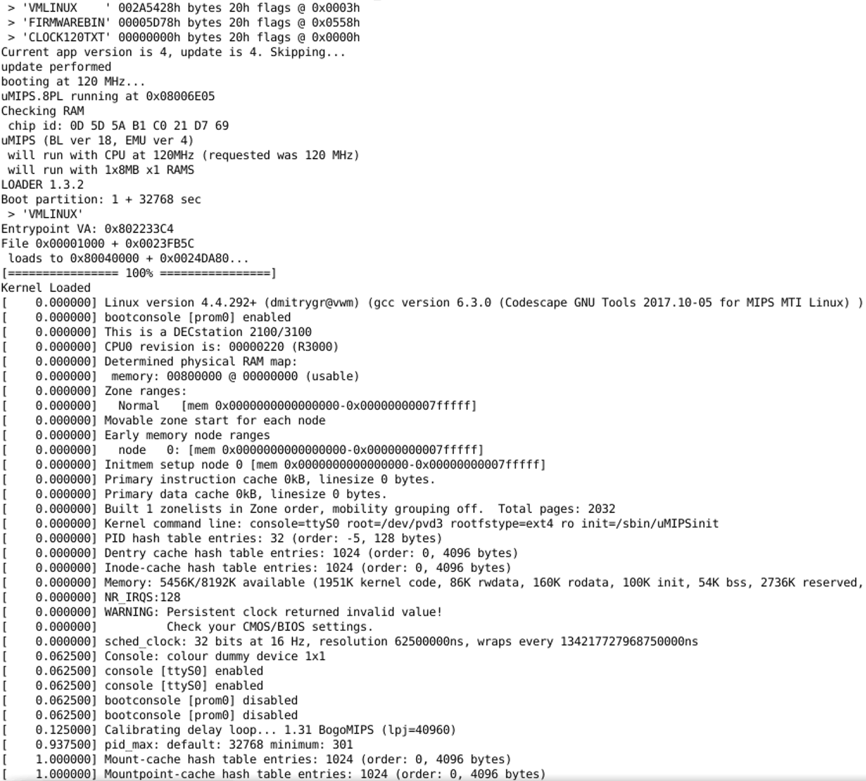
Same as in my previous MIPS-emulating projects, the boot process is reminiscent of the PC boot process. The first sector of the card is read into the first bytes of RAM and jumped to. It may then load the next stage. It does so by looking for a partition with type 0xBB and loading it into ram at address 0x80001000 and then jumping to it. There, lives the second-stage bootloader. It is large enough to contain logging and console output. It will look for a partition marked as active, attempt to mount it as FAT16, and find a file there called VMLINUX. If it is found, it is loaded as an ELF file and its entry point is jumped to. If this is a valid Linux kernel, it will then boot. The commandline passed to the kernel is embedded in the bootloader since it is not expected to change. It instructs the kernel to mount /dev/pvd3 as root and use /sbin/uMIPSinit as init. It will try to mount /dev/pvd1 as /boot
A careful read of the above paragraph would show that while the rootfs needs to be the third partition, no other order is specified or matters. This is on purpose. For this project, the FAT partition is first, the bootloader partition second, and rootfs third. Why? When an SD card with multiple partitions is inserted, Windows and macOS will mount the first partition. Linux will mount them all. This means that (1) the FAT partition can be used to easily get files in and out of this machine as they are also visible to the booted Linux in /boot and (2) clock speed changing/overclocking is easy from the host machine and/or from the booted Linux itself.
The first thing the bootloader does is simply wait six seconds without doing anything. This is done before reconfiguring the pins. The delay allows for some time to attach an SWD debugger, if so desired (the board has a 4-pin header for that). After this delay, the pins are reconfigured and there are no more pins assigned to SWD, and thus a debugger cannot be attached anymore. As a secondary backup, the bootloader configures the option bytes to allow forcing the chip to boot from ROM by raising the BOOT0 pin (pin 8). It also programs the option bytes to disable the reset pin (it is being used as a GPIO) and to disable the BOR (it is of no use here). Then it will try to initialize comms with the SD card and check for updates, then it will boot.
Performance
STM32G031 is specified to run at 64MHz, so why all this talk about running it at 150MHz? Well, with the proper application of dark magic, STM32G031 overclocks quite well. The CPU core runs from an internal regulator whose voltage is adjusted using the PWR->CR1 register. STM documents two settings: VOS2 (corresponding to Vcore of 1.0V) where the chip can only be run up to 16MHz and VOS1 (corresponding to Vcore of 1.2V) where the chip can only be run up to 64MHz. Indeed, at VOS1, the chip will not run well past about 75MHz. A respectable overclock, but not that exciting. However.... older documentation (and documentation of similar chips) also mentions VOS0, corresponding to Vcore of 1.35V. What if one tries? Well, what do you know? It works, and the chip gets a LOT more overclockable. Now, most instances of the chip run well at 136MHz, and some get to 180MHz. You do need to manage the flash wait states correctly, since the flash memory will not magically get any faster. The extra wait states do eat into the speed gains, but it is still worth it.
At 148MHz host CPU speed, the emulated MIPS CPU is approximately equivalent to a 1.65MHz MIPS R3000 with FPU disabled. It is not a speed beast, but it does boot in about a minute, and things like vi, make, objdump, and gcc work. This is a full Debian system, so you can bring in .deb packages via /boot and install them even. It all works.
Assembly
Acquisition
You can buy the parts yourself and get a board made by your favourite board house (all the things you need are in the downloads below), or (I hope) you'll be able to buy a kit soon. I am looking for a company that wants to sell the kit. Contact me if you have a lead on this. They would make great gifts!
Initial assembly
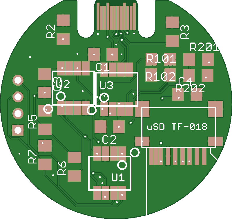
The part you came here for: how to build your own. Here you see the board you are likely holding in your hands. It is pretty easy to assemble, and this is by design. The first thing you solder in should be the SD card socket. Line it up carefully in the box and solder the pins one at a time, then solder the four corner pads that hold it to the board. These take a bit more heat so be patient. Next, solder in all the capacitors. There are four and they are all the same value so it is easy. They go into slots labeled C1 through C4. Next up, solder in all the resistors. They are also all the same value for ease of assembly. They go into places labeled R2 through R7 (there is no R4). Do not fill in slots R101, R102, R201, and R202 yet.
Next up, solder in the microcontroller (STM32G031J6). It goes into the place labeled U1. Direction matters here. On these, the first pin is labeled by a little image of the STM logo. On the board, pin 1 is labeled using a small circle inside the outline as well as outside of it. Rotate the chip correctly and solder it in. Next, solder in the USB-to-serial chip (PL2303GL). It goes into the slot labeled U3. On this chip, pin one is indicated by a little dimple in the corner on top of the chip. Line that up with the board's pin 1 marker and solder it in.
Secondary assembly
At this point in time, you must program the bootloader into the microcontroller. To do this, use STM's "flasher" utility. You'll need a USB-C cable. To connect the proper pins to the serial port, you'll need to use two pieces of wire (or just solder) to bridge the places labeled R101 and R201 on the board. Make sure you do not have an SD card inserted into the onboard socket and you did not yet solder-in the RAM chip. Then, plug the cable into your computer and insert the board carefully into the USB-C end of the cable. The PC should detect a virtual serial port and install drivers automatically. Now you'll need the flasher utility. You may get it here for windows. There is an open-source alternative with other platform support here. If you build that tool, the process is the usual one: ./configure && make. Using it is easy too: ./stm32flash -w BOOTLOADER.BIN -v /dev/ttyUSB0, assuming those names and paths are correct for your use case. If you have an SWD debugger you may instead use it to program the bootloader into the chip. From the download package, grab "BOOTLOADER.BIN" and have that programmed into the chip.
At this point, remove the solder bridges or wires you used to bridge R101 and R201 and instead bridge R102 and R202. This is the proper final configuration for the serial port pins. Solder in the RAM chip now (APS6408 or VTI7064), marked U2. Pin 1 on this chip is also marked with a small dimple. Match that up with the small circle on the board and solder the chip in. This concludes the hardware assembly.
Flashing the main firmware and first boot
Use a disk imaging tool (WIN32 DISK IMAGER for windows, built-in "Disk Utility" for macOS, dd for Linux) to write the provided disk image unto an SD card of at least 1GB in size. This image includes the first-stage MIPS bootloader, the second-stage MIPS bootloader, a partition with the Linux kernel and a copy of the firmware, and a debian rootfs. After the card is written, eject it and reinsert it. Your PC should now recognize the FAT filesystem and mount it. Drop the main firmware into it from the download package, named FIRMWARE.BIN. This will allow the bootloader to pick it up and self-flash it on first boot. This step is not necessary if you did not rebuild it, as the provided image already contains that file there. It is, however, safe to do it anyways. You're done!
Insert the SD card, connect the cable to the PC again, open your favourite serial terminal, and configure it for 115,200 bps, 8N1. After a few seconds you'll see text appear as the various stages of bootloaders run. The very first time, STM32's fuses will be programmed and you may need to unplug and replug the USB-C cable to continue the boot process. This will only need to happen once since the fuses are nonvolatile. After about 20 seconds, the Linux kernel boot messages will start. The boot process will take about a minute. At the end you'll end up at a shall prompt. As there is only 8MB of RAM, making swapon /swapfile your first command is strongly suggested. This will take a few dozen seconds to complete, but after it you'll have swap and ability to run a lot more things. Play around. Enjoy!
Downloads and Use
The files
The main download is [here]. That is an archive that contains everything you need. The schematics directory contains the schematics, gerbers contains the gerbers you'd need to have boards made, and srcs contains the sources of the emulator and the bootloader. In the binaries directory you'll find the SD card image (SD.img) that you'll want to write directory to your card, BOOTLOADER.BIN is the bootloader you'll write to the chip in the middle of assembling the project, and FIRMWARE.BIN is a pre-built firmware image (a copy of which is already in SD.img's first partition).
Using it
The device boots to a shell prompt using sh. You may start bash if you wish - it works. To not run out of RAM, as mentioned above, it is advisable to enable swap. A pre-made swapfile is in the image, simply run swapon /swapfile as one of your first commands. The effective CPU speed is about 1.5MHz assuming you're running the MCU at 120MHz, so go keep in mind that commands will take time. Compiling a simple program with gcc will take a few minutes, but it will work. Provided examples include two Mandelbrot set generators (floating point and fixed point), compiled and binary both.
The usual tools are installed: vim, make, and gcc. All the usual debian packages are there too, and you can load more things using the shared FAT16 partition on the SD card. Under Linux it is mounted under /boot
Comments...
